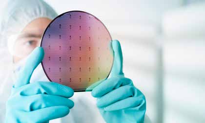
Bringing a wealth of knowledge and problem solving skills in semiconductor wafer surfacing, wafer thinning (back lapping) and geometric control.
Our team of experts will work with you to integrate the relevant processes and systems into your thin or ultra thin wafer fabrication programme. Initial discussions provide a detailed understanding of production quantity, wafer thickness, surface finish and geometric tolerance requirements.
Having over 50 years experience in design and manufacture of high precision equipment and in sophisticated materials processing, we provide a quick and effective route to complete success in any device fabrication process.
Application Analysis
Our systems are typically used in the processing of:
Silicon
Gallium Arsenide
Cadmium Zinc Telluride
Indium Phosphide
Mercury Cadmium Telluride
Cadmium Sulphide
A Logitech system for semiconductor wafer processing typically includes:
- Wafer-support disc bonding of low, medium or high precision
- Jig controlled lapping and polishing using automated single, single or multi-workstation machines
- Mild Chemical Mechanical Processing (CMP) or aggressive chemical etch polishing within a controlled environment
- CMP processing using a dedicated system, such as a Logitech High Speed System, Tribo or Orbis system
- Gauging and inspection facilities to suit the required end result.
Suggested Links
Call me back
To speak to one of our technical experts, fill this form out and we will get back to you.