Logitech Labs : Copper
30th October 2020
Here at Logitech we are dedicated to continuous development and improvement for the benefit of our customers.
Our lab team with over 50 years of combined experience, work with our customers and their samples to ensure the most up-to-date and advanced process techniques are available to help get the most out of their processes.
Whether it be continuous research and development to ensure we are up to date with the latest technologies and process knowledge or continuing to develop our existing products, we are always moving to improve.
Below is an example of copper samples in our lab this week:
Copper
In recent weeks, our laboratory in Logitech have been successful in processing electroplated Copper wafers by planarising back to a barrier layer. This week the wafers have undergone various device depositions, and copper plating layers where the copper plating has been planarised for each layer using the Logitech CMP Orbis machine.
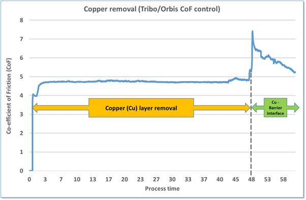
So whether the copper is a plain plated layer or part of through-silicon vias (TSV’s) or through-glass vias (TGV’s) then our CMP Tribo and CMP Orbis systems can provide a high level of performance ready for next device processes. In addition the intelligent drive system provides reliable end point detection via co-efficient of friction (CoF) tracking for a given process setup condition.
An example of the CoF output data can be seen in the chart provided.
Our dedicated process team are always on hand, on-site, or reachable by email, to offer further advice and problem solving knowledge.
If interested in more detail contact us on +44 (0)1389 875444 or enquiries@logitech.uk.com to learn more about the difference we can make to your processes.


