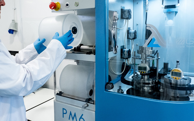
Extranet Login

t: +44 (0)1389 875444|e:enquiries@logitech.uk.com

  • Who we are
    • Our History
    • Quality & Accreditations
    • Our Environmental Policies
      • Our WEEE Policy
    • Careers
  • What we offer
    • By application
      • Semiconductors
      • Geological Sciences
      • Optoelectronics
      • Optics
      • Other applications
    • By material
      • Silicon
      • Silicon Carbide
      • Sapphire
      • Gallium Arsenide
      • Cadmium Zinc Telluride
      • Indium Phosphide
      • Rock/Soil
      • Other Materials
  • Products & Solutions
    • Lapping & Polishing
    • Chemical Polishing & Chemical Mechanical Polishing
    • Driven Head Lapping & Polishing Tools
    • Bonding & Impregnation Units
    • Test & Measurement
    • Cutting & Sawing
    • Accessories
    • Consumable Items
    • Consumables Store
  • Knowledge base
    • Whitepapers
    • Tech Files – Blog
    • Technology Transfer Programme
    • Brochures
    • Application Process Notes
    • Case Studies
    • FAQ
  • News & Events
    • News
    • Events
  • Contact
    • How to find us
    • Global Distributors
    • Equipment Returns
Menu
  • Who we are
    • Our History
    • Quality & Accreditations
    • Our Environmental Policies
      • Our WEEE Policy
    • Careers
  • What we offer
    • By application
      • Semiconductors
      • Geological Sciences
      • Optoelectronics
      • Optics
      • Other applications
    • By material
      • Silicon
      • Silicon Carbide
      • Sapphire
      • Gallium Arsenide
      • Cadmium Zinc Telluride
      • Indium Phosphide
      • Rock/Soil
      • Other Materials
  • Products & Solutions
    • Lapping & Polishing
    • Chemical Polishing & Chemical Mechanical Polishing
    • Driven Head Lapping & Polishing Tools
    • Bonding & Impregnation Units
    • Test & Measurement
    • Cutting & Sawing
    • Accessories
    • Consumable Items
    • Consumables Store
  • Knowledge base
    • Whitepapers
    • Tech Files – Blog
    • Technology Transfer Programme
    • Brochures
    • Application Process Notes
    • Case Studies
    • FAQ
  • News & Events
    • News
    • Events
  • Contact
    • How to find us
    • Global Distributors
    • Equipment Returns
Home  /  View our Lapping & Polishing Systems  /  PM6 Precision Lapping & Polishing System

PM6 Precision Lapping & Polishing System

Categories: View All, View our Lapping & Polishing Systems
  • PM6 Precision Lapping & Polishing System
  • PM6 Lap and Polish System
  • PM6 Lapping machine
  • PM6 Precision Lapping & Polishing System
  • PM6 Lap and Polish System
  • PM6 Lapping machine

Product Video:

  • Description
  • Additional information
  • Facilities Requirement
  • Applications
  • Accessories & Consumables

Description

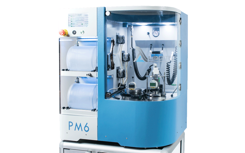
The PM6 Precision Lapping & Polishing system produces results typically found on production scale equipment. Highly flexible in use, the PM6 allows users to work with many different materials including; gallium arsenide, silicon, rock and soils. This system provides the ability to produce specimens repeatably with superior quality and surface
finish. Precise plate set-up options combined with an intuitive control system provide an effortless consistency of results with a very high degree of accuracy.

Wherever there is a need for a controlled flat surface with a high quality finish the PM6 makes an invaluable investment. The PM6 system offers enhanced process performance through a combination of innovative designs and intuitive operator
controls.

  • Single workstation with a wafer process capacity of up to 4”/100mm – driven jig roller arms greatly increases accuracy and repeatability.
  • Plate speeds of between 5 and 100rpm, which facilitates faster lapping and polishing rates.
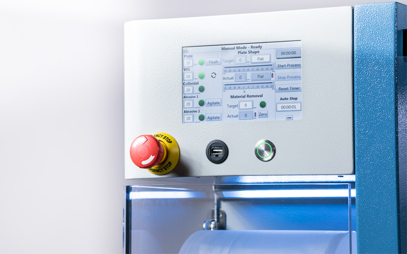
  • The recipe mode feature allows operators to create, save and re-call multi-stage process recipes.
  • The metered abrasive feed unit, via the peristaltic pumps, allows operators to set the flow rate of between 1-100ml per minute. This greatly increases the quality and the accuracy of results, while reducing both wastage and operational costs.
  • Customers are achieving increased material removal rates (MRR), with far greater control, compared to similar systems without metered abrasive delivery or a driven-jig-arm functionality.
  • All process conditions are controlled via the Graphical User Interface (GUI), including: plate speeds, material removal rates, driven jig arm, the metered abrasive feed – giving the operator complete control.
  • The automatic drip detector will stop the plate rotating when the abrasive cylinders are empty – thereby avoiding any damage to the specimen running on a dry plate.
  • Real time data collection and feedback via Bluetooth to allow users to export information via the USB port for external analysis.
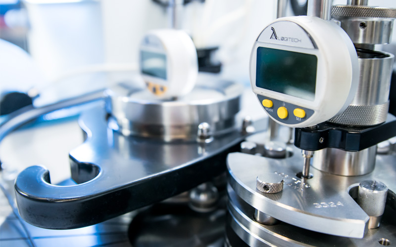
  • Bluetooth automatic-plate-flatness control provides continuous in-situ measurement of the plate flatness.
Download Brochure

Key Features

  • Process up to 100mm/4″ wafers
  • Up to 100rpm plate speed facilitating faster lapping rates
  • Driven jig roller arm with linear sweep
  • Bluetooth enabled features
  • Automatic plate flatness control


Customer Review

“There have been a lot of new and used machines I have operated before. The PM6 is first machine on which we can actually start producing real parts after 4 days of training. When we were expanding our business, I did not think about anyone else, I called Logitech.” 

Guofeng Pang – Senior Developer, Engineer

Additional information

video

https://youtu.be/NZ7aTx4hOOw

Power Supply 220-240v 10A

110v 10A

50-60HZ

Jig type PP5(x1) PP6(x1)
Plate speed 5-100 rpm
Plate sizes

(diameter)

300mm


Height

(including extraction port)

915mm

965mm

Depth 720mm
Width 802mm
Mass

(Excluding cylinders etc)

127kg
Plate Flatness Monitor

(Bluetooth enabled)

0.1 Micron Resolution
Abrasive Delivery Up to 2x 2L Cylinders,

Measured flow


Peristaltic pump

1-100ml/min

Colloidal Delivery Peristaltic pump

1-100ml/min

Geological Sciences

geologicalsciences

In many areas of geological study such as mineralogy, petrography and sedimentology you are required to analyse the characteristics of the materials such as soil or rock.  To be able to do this a thin section needs to be prepared for microscopic examination.

Logitech precision equipment is ideal for thin or ultra-thin section preparation.  Our wide range of versatile systems enable you to trim, lap and polish geological thin sections such as rock, coal, concete and soils.

Each of our systems are fully supported by a wide range of accessories and consumables, such as abrasive powders, polishing cloths and mounting media.

Semiconductors

semiconductors

Semiconductor materials are used in a wide variety of devices such as field effect transistors (MosFets, Fets), integrated circuits (ICs, MMICs, ASICs), focal plane arrays and infra-red detectors.

Whatever the application or material, each semiconductor wafer undergoes several common stages during manufacture, which include slicing the wafer from the crystal, preparing the surface prior to fabrication and thinning the device after fabrication through the use of lapping and polishing techniques.

Logitech provide complete system solutions including consumables for the precise thinning of these III-V, I.R. and similar materials.

CMP Applications

Primary applications areas are in the field of Tribology Science and Research, particularly with regards process and analysis results.  For example co-efficient of friction monitoring (CoF).

The Tribo chemical mechanical polishing system is also readily adaptable as an enabling technology in Microelectromechanical Systems (MEMS) fabrication, particularly polysilicon surface micromachining, Opto-MEMS and Bio-MEMS packaging, assembly and even fabrication.

Optoelectronics

optoelectronics

Advances in communication technology have led to the development of a wide variety of optoelectronics and integrated optics devices for applications such as; dense wavelength division multiplexing (DWDM), optical isolators, signal processors and optical switching.

Logitech has a large selection of adaptable systems for the preparation of optoelectronic materials such as; silicon, lithium niobate, lithium tantalate, bismuith silicon oxide, barium titanate and similar materials.

Our systems, accessories and consumables provide defect free face and edge polishing on optoelectronic substrate and scratch free surfaces with exacting and repeatable dimensional tolerances.

Optics

optics

The importance of optical polishing and the processing of optical components has never been greater with the ongoing development of the telecommunications market. Whether for Infra Red and polymer waveguide production or fibre optic cable polishing.

The precision design and manufacture of our equipment enable you to obtain maximum results from the cutting, lapping and polishing of these optical materials.

Other Applications

otherapplications

Logitech systems are used by organisations across the world for many different complex sample preparation processes.

Including the thin section preparation of; Teeth, Bone, Otoliths, Ceramics, Metals, Alloys, Polymers and other Carbon-based materials.


Lapping Plates

lappingplates

The Logitech range of lapping plates provides a comprehensive selection for lapping of a wide range of materials.

Polishing Plates

polishingplates

The Logitech range of polishing plates provides a comprehensive selection for polishing a wide range of materials.

Abrasive Autofeed Cylinder

abrasiveautofeedcylinder

Abrasive autofeed cylinder for use with a Logitech PM5 or LP50 system.  Cyclinders are also available in a sodium hypochlorite resistant material, for use with Chemical Mechanical Polishing applications.

Weights and Pressure Blocks

weightsandpressureblocks

Logitech supply weights and pressure blocks for use with Logitech lapping systems.

Conditioners/Test Blocks

conditionerstestblocks

We supply a range of cast iron and glass test blocks as well as cast iron, glass and diamond conditioners for your lapping applications.

EP Polishing Pads and Cloths

Logitech EP1 and EP2 Chemical Mechanical Polishing (CMP) Polishing Cloths and pads are suitable for a wide range of applications.  Including oxide, nitride and copper.

Geochem Polishing Cloths

geochempolishingcloths

Logitech Geochem Polishing Cloths are ideal for geological or semiconductor III-V material polishing.

IC1000 & Suba Polishing Pads and Cloths

Logitech IC1000 pads and Suba felts are specifically designed for stock and intermediate polishing where achieving a high precision surface is critical.  They can be used across a wide range of materials including; GaAs, silicon, glass, metals, quartz, ceramics, copper and diamond thin film.

Aluminium Oxide Powder

Calcined Aluminium Oxide powders for lapping and polishing hard materials.

Silicon Carbide Powders

For use in high precision lapping and polishing operations. Available in a wide range of grit sizes.

Fused Aluminium Oxide Powder

Fused Alumium Oxide powders for precision lapping and optical polishing operations.

Carrier Disc & Substrates

Logitech glass carrier discs are used for the temporary support of both semiconductor and opto-electronics wafers during thinning and polishing operations.

Cleaning Fluids & Powders

Logitech cleaning fluids and powders and non-solvent based.  They are suitable for most sample and substrate cleaning applications, including demounting of ultra-thin semiconductor wafers.

the-tech-files

Expert news and views to help sharpen your cutting edge

DIAMONDS ARE AN ENGINEER’S BEST FRIEND

In recent years, diamond has emerged as not only a girl’s best friend, but also as contender as an engineer’s best friend – if the technical challenges of exploiting its remarkable properties can be overcome.

LOGIN TO VIEW

THE END OF THE CHIP FOR SILICON?

Silicon-based semiconducting integrated circuits have changed the world immeasurably over the past 50 years. Today the number of silicon chips in use far outweighs the number of humans currently alive.

LOGIN TO VIEW

OPTIMAL FRICTION FOR OPTIMAL FLATNESS

The wafers used to make semiconducting chips for electronic devices all have one thing in common – they need to be smooth – super smooth. Typically, wafer flatness needs to be controlled within ±2 μm.

FREE TO VIEW
contact-us-icon
contact-us-icon
contact-us-icon

Home  |  Sitemap  |  Privacy Policy  | Cookies Policy | Environmental Policy | Contact Us  |  Extranet | Indicor

We are using cookies to give you the best experience on our website.

You can find out more about which cookies we are using or switch them off in .

Powered by  GDPR Cookie Compliance
Privacy Overview

This website uses cookies so that we can provide you with the best user experience possible. Cookie information is stored in your browser and performs functions such as recognising you when you return to our website and helping our team to understand which sections of the website you find most interesting and useful.

Strictly Necessary Cookies

Strictly Necessary Cookie should be enabled at all times so that we can save your preferences for cookie settings.

If you disable this cookie, we will not be able to save your preferences. This means that every time you visit this website you will need to enable or disable cookies again.