Optimal friction for optimal flatness
25th August 2015
 The wafers used to make semiconducting chips for electronic devices all have one thing in common – they need to be smooth – super smooth.
Typically, wafer flatness needs to be controlled within ±2 μm across the entirety of the wafer.
Achieving such controlled levels of flatness reproducibly requires an intimate understanding of how the wafer interacts with the pad and slurry during chemical mechanical polishing (CMP) processes.
To gain this information a system that can analyse and process removal rates in real time is needed. In addition it needs to relay information such as end point detection (EPD) and process stability back to the operator in real-time so that consistent and repeatable performance is attainable.
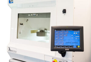
Incorporating cutting edge technology, such as advanced process sensors, diamond pad conditioning and a modular component structure, Logitech’s Tribo system has been designed to add a sparkle to CMP research and analysis.
The Tribo system provides researchers with the ability to process coupons, part wafers and full wafers of up to 4″/100mm in diameter on a 400mm polishing plate. A second driven carrier arm allows for various in-situ pad conditioners to be mounted while a 4.25″ diamond pad conditioner maintains the original properties of the polishing pad and minimises wafer-to-wafer variations.
Various system operations can be precisely automated to enable entire CMP processes to be initiated and then left unmanned. This allows the operator to work on other tasks safe in the knowledge that the Tribo is automatically performing the specified processes and monitoring the results.
Detailed insight provides great reliability, increased wafer yields, greater process reliability and a lower cost of ownership.
To learn more about the Tribo, simply click here.