How to soften the challenge of finishing silicon carbide
29th April 2015
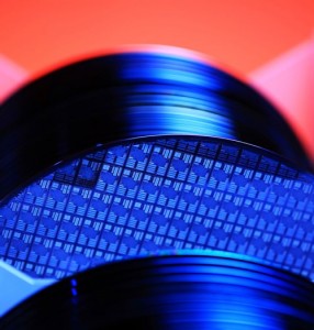 Silicon Carbide (SiC or carborundum) has become the material of choice in applications ranging from fibre optics and LEDs to power electronics. Devices based upon SiC can operate at a higher temperature, power level and voltage than other materials. This in turn enables improved energy efficiency in SiC-based power devices, LED lighting and telecommunications.
However, the production of defect-free wafers of SiC has proven a challenge and to-date, the majority of SiC device work is based on 76mm and 100mm diameter substrates. This increases the manufacturing costs as the die count per wafer is lower.
To complicate matters further, SiC is one of the hardest materials known to mankind, and this makes lapping and polishing SiC wafers a time-consuming and laborious challenge without the right equipment.
While material removal rates can be improved using advanced slurries and technology, the inherent hardness of these wafer materials means that cycle times are slower than for standard silicon for example. As a consequence, it is vital that automated technology is deployed for polishing and lapping as this will allow the machine to run unattended, thus negating labour costs.
To learn more about how automated finishing systems can improve process flows for SiC-based devices, download our whitepaper.