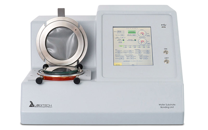
Extranet Login

t: +44 (0)1389 875444|e:enquiries@logitech.uk.com

  • Who we are
    • Our History
    • Quality & Accreditations
    • Our Environmental Policies
      • Our WEEE Policy
    • Careers
  • What we offer
    • By application
      • Semiconductors
      • Geological Sciences
      • Optoelectronics
      • Optics
      • Other applications
    • By material
      • Silicon
      • Silicon Carbide
      • Sapphire
      • Gallium Arsenide
      • Cadmium Zinc Telluride
      • Indium Phosphide
      • Rock/Soil
      • Other Materials
  • Products & Solutions
    • Lapping & Polishing
    • Chemical Polishing & Chemical Mechanical Polishing
    • Driven Head Lapping & Polishing Tools
    • Bonding & Impregnation Units
    • Test & Measurement
    • Cutting & Sawing
    • Accessories
    • Consumable Items
    • Consumables Store
  • Knowledge base
    • Whitepapers
    • Tech Files – Blog
    • Technology Transfer Programme
    • Brochures
    • Application Process Notes
    • Case Studies
    • FAQ
  • News & Events
    • News
    • Events
  • Contact
    • How to find us
    • Global Distributors
    • Equipment Returns
Menu
  • Who we are
    • Our History
    • Quality & Accreditations
    • Our Environmental Policies
      • Our WEEE Policy
    • Careers
  • What we offer
    • By application
      • Semiconductors
      • Geological Sciences
      • Optoelectronics
      • Optics
      • Other applications
    • By material
      • Silicon
      • Silicon Carbide
      • Sapphire
      • Gallium Arsenide
      • Cadmium Zinc Telluride
      • Indium Phosphide
      • Rock/Soil
      • Other Materials
  • Products & Solutions
    • Lapping & Polishing
    • Chemical Polishing & Chemical Mechanical Polishing
    • Driven Head Lapping & Polishing Tools
    • Bonding & Impregnation Units
    • Test & Measurement
    • Cutting & Sawing
    • Accessories
    • Consumable Items
    • Consumables Store
  • Knowledge base
    • Whitepapers
    • Tech Files – Blog
    • Technology Transfer Programme
    • Brochures
    • Application Process Notes
    • Case Studies
    • FAQ
  • News & Events
    • News
    • Events
  • Contact
    • How to find us
    • Global Distributors
    • Equipment Returns
Home  /  Bonding & Impregnation Units  /  WSBU Wafer Substrate Bonding Units

WSBU Wafer Substrate Bonding Units

Categories: Bonding & Impregnation Units, View All
  • WSBU Wafer Substrate Bonding Units
  • WSBU Wafer Substrate Bonding Units

Product Video:

  • Description
  • Facilities Requirement
  • Applications
  • Accessories & Consumables

Description

The Logitech Wafer Substrate Bonding Units (WSBU’s) offer premium bonding for the processing of fragile semiconductor materials such as indium phosphide and gallium arsenide. The bonding units are designed to minimise breakage with these expensive materials, whilst retaining the highest quality of sample yield.

The WSBU’s are designed to meet the stringent requirements of todays wafer processes. Available as a single, three station, or floor standing model, this highly automated bonder incorporates both vacuum and pressure bonding facilities.

Available as a single or three station benchtop unit with a wafer process capacity of 4”/100mm or 6”/150mm – bond three part or whole wafers consistently with a high standard of support carrier parallelism.

The WSB300 floor standing model allows operators to bond materials and wafers up to 300mm/12” (or smaller multiple samples using a template) in diameter to the exacting standards achieved by the benchtop WSBU’s
– this makes the WSB300 ideal for high throughput bonding requirements.

Our latest environmentally conscious upgrade: the 12” bonder now features an updated cooling system, replacing the oil-based heat exchangers.

Dry pump option now available upon request, completely eliminating reliance on oil-based products. This means not only enhanced performance but also a significant reduction in our environmental footprint.

Visit our Online Consumables store

Download Brochure

Key Features

  • 100mm (4″), 150mm (6″) or 300mm (12″) wafer capacity
  • Single or multiple wafer bonding
  • Process repeatability
  • Automated process cycle
  • Excellent wafer to support disc parallelism
  • Now with updated software to further meet your process demands.

Product Specifications:

Single Station
100mm (4″)
Single Station
150mm (6″)
Three Station
100mm (4″)
Three Station
150mm (6″)
Single Station
300mm (12″)
Power Supply: 240v/110v Single Phase 240v/110v Single Phase 240v/110v Single Phase 240v/110v Single Phase 240v Single Phase
Water Supply:                                        Mains Pressure Cold Water
Pressurised Air (optional):                                          Regulated to 2bar ± 0.2bar maximum                           5-8 Bar
Height:  345mm   400mm   345mm   370mm  1740mm
Depth:  580mm  600mm  580mm  600mm 750mm
Width:   520mm*  740mm*   940mm*  1160mm*       1185mm**
Weight:  30kg  30kg  110kg  100kg 320kg
Vacuum Pump (RV3): Single Station WSBU 4” – RV3 pump or nXDS6i Pump
Single Station WSBU 6” / Triple Station WSBU 4” & 6” / Single Station WSB300 12”
RV8 pump or nXDS10i Pump

Vacuum Level in all bonding chambers during bonding sequence <0.1mbar

*Add 200 mm for services pipework
** Includes Services

Semiconductors

semiconductors

Semiconductor materials are used in a wide variety of devices such as field effect transistors (MosFets, Fets), integrated circuits (ICs, MMICs, ASICs), focal plane arrays and infra-red detectors.

Whatever the application or material, each semiconductor wafer undergoes several common stages during manufacture, which include slicing the wafer from the crystal, preparing the surface prior to fabrication and thinning the device after fabrication through the use of lapping and polishing techniques.

Logitech provide complete system solutions including consumables for the precise thinning of these III-V, I.R. and similar materials.

Optoelectronics

optoelectronics

Advances in communication technology have led to the development of a wide variety of optoelectronics and integrated optics devices for applications such as; dense wavelength division multiplexing (DWDM), optical isolators, signal processors and optical switching.

Logitech has a large selection of adaptable systems for the preparation of optoelectronic materials such as; silicon, lithium niobate, lithium tantalate, bismuith silicon oxide, barium titanate and similar materials.

Our systems, accessories and consumables provide defect free face and edge polishing on optoelectronic substrate and scratch free surfaces with exacting and repeatable dimensional tolerances.

Optics

optics

The importance of optical polishing and the processing of optical components has never been greater with the ongoing development of the telecommunications market. Whether for Infra Red and polymer waveguide production or fibre optic cable polishing.

The precision design and manufacture of our equipment enable you to obtain maximum results from the cutting, lapping and polishing of these optical materials.

Heat Transfer

Logitech Heat Transfer is a cooling oil for use with a Logitech WSBU system.

Mounting Adhesives

Logitech provides a range of mounting media for bonding of semiconductor, optic and geological samples.

Glass Microscope Slides

Logitech glass microscope slides are used for the permanent mounting of thin rock, concrete and soil thin sections.

Glass Slide Coverslips

Glass coverslips protect valuable thin sections and improve optical clarity for transmitted microscopy.

the-tech-files

Expert news and views to help sharpen your cutting edge

DIAMONDS ARE AN ENGINEER’S BEST FRIEND

In recent years, diamond has emerged as not only a girl’s best friend, but also as contender as an engineer’s best friend – if the technical challenges of exploiting its remarkable properties can be overcome.

LOGIN TO VIEW

THE END OF THE CHIP FOR SILICON?

Silicon-based semiconducting integrated circuits have changed the world immeasurably over the past 50 years. Today the number of silicon chips in use far outweighs the number of humans currently alive.

LOGIN TO VIEW

OPTIMAL FRICTION FOR OPTIMAL FLATNESS

The wafers used to make semiconducting chips for electronic devices all have one thing in common – they need to be smooth – super smooth. Typically, wafer flatness needs to be controlled within ±2 μm.

FREE TO VIEW
contact-us-icon
contact-us-icon
contact-us-icon

Home  |  Sitemap  |  Privacy Policy  | Cookies Policy | Environmental Policy | Contact Us  |  Extranet | Indicor

We are using cookies to give you the best experience on our website.

You can find out more about which cookies we are using or switch them off in .

Powered by  GDPR Cookie Compliance
Privacy Overview

This website uses cookies so that we can provide you with the best user experience possible. Cookie information is stored in your browser and performs functions such as recognising you when you return to our website and helping our team to understand which sections of the website you find most interesting and useful.

Strictly Necessary Cookies

Strictly Necessary Cookie should be enabled at all times so that we can save your preferences for cookie settings.

If you disable this cookie, we will not be able to save your preferences. This means that every time you visit this website you will need to enable or disable cookies again.