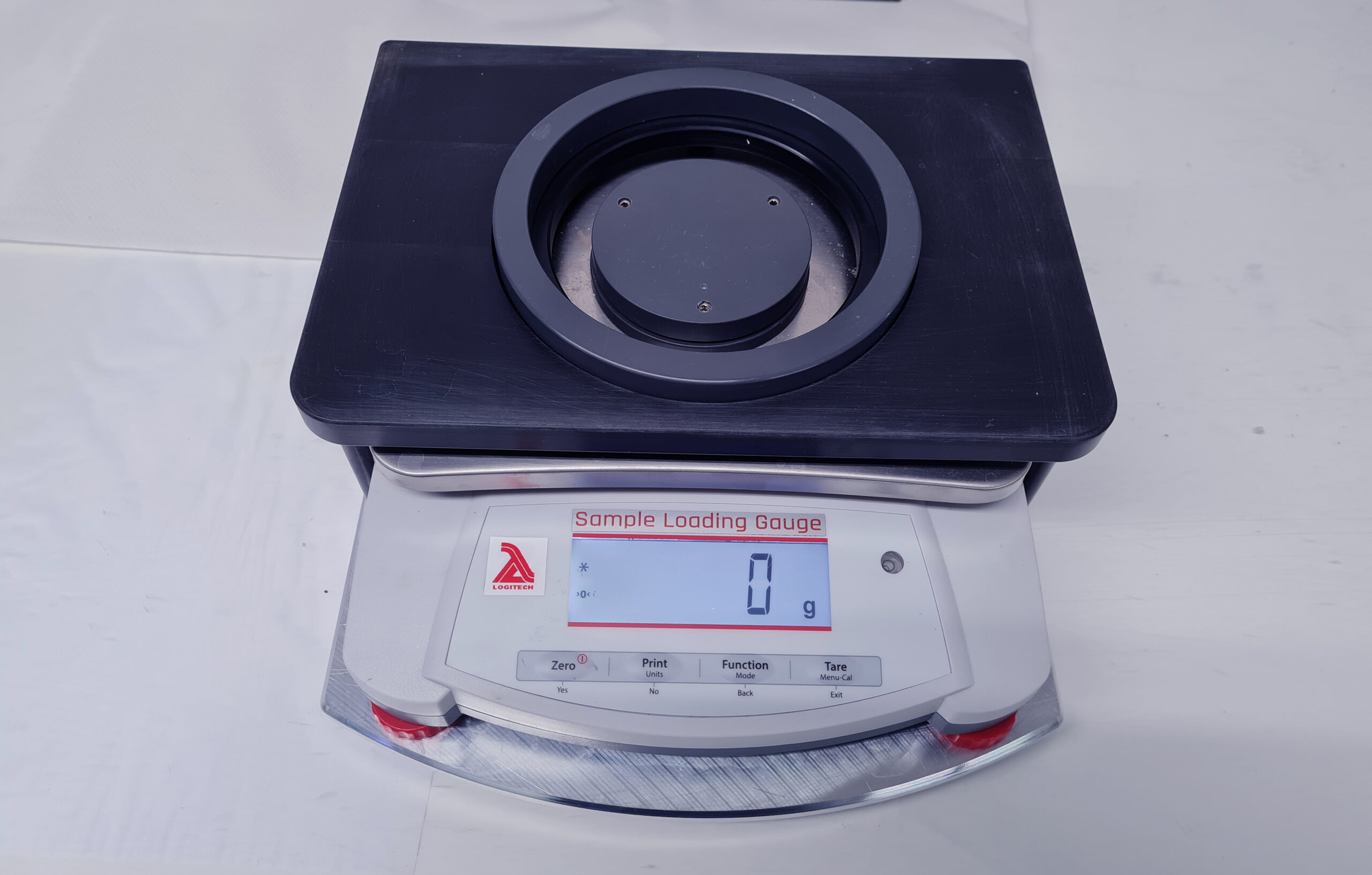
Extranet Login

t: +44 (0)1389 875444|e:enquiries@logitech.uk.com

  • Who we are
    • Our History
    • Quality & Accreditations
    • Our Environmental Policies
      • Our WEEE Policy
    • Careers
  • What we offer
    • By application
      • Semiconductors
      • Geological Sciences
      • Optoelectronics
      • Optics
      • Other applications
    • By material
      • Silicon
      • Silicon Carbide
      • Sapphire
      • Gallium Arsenide
      • Cadmium Zinc Telluride
      • Indium Phosphide
      • Rock/Soil
      • Other Materials
  • Products & Solutions
    • Lapping & Polishing
    • Chemical Polishing & Chemical Mechanical Polishing
    • Driven Head Lapping & Polishing Tools
    • Bonding & Impregnation Units
    • Test & Measurement
    • Cutting & Sawing
    • Accessories
    • Consumable Items
    • Consumables Store
  • Knowledge base
    • Whitepapers
    • Tech Files – Blog
    • Technology Transfer Programme
    • Brochures
    • Application Process Notes
    • Case Studies
    • FAQ
  • News & Events
    • News
    • Events
  • Contact
    • How to find us
    • Global Distributors
    • Equipment Returns
Menu
  • Who we are
    • Our History
    • Quality & Accreditations
    • Our Environmental Policies
      • Our WEEE Policy
    • Careers
  • What we offer
    • By application
      • Semiconductors
      • Geological Sciences
      • Optoelectronics
      • Optics
      • Other applications
    • By material
      • Silicon
      • Silicon Carbide
      • Sapphire
      • Gallium Arsenide
      • Cadmium Zinc Telluride
      • Indium Phosphide
      • Rock/Soil
      • Other Materials
  • Products & Solutions
    • Lapping & Polishing
    • Chemical Polishing & Chemical Mechanical Polishing
    • Driven Head Lapping & Polishing Tools
    • Bonding & Impregnation Units
    • Test & Measurement
    • Cutting & Sawing
    • Accessories
    • Consumable Items
    • Consumables Store
  • Knowledge base
    • Whitepapers
    • Tech Files – Blog
    • Technology Transfer Programme
    • Brochures
    • Application Process Notes
    • Case Studies
    • FAQ
  • News & Events
    • News
    • Events
  • Contact
    • How to find us
    • Global Distributors
    • Equipment Returns
Home  /  Accessories  /  Sample Loading Gauge

Sample Loading Gauge

Category: Accessories
  • Description
  • Facilities Requirement
  • Applications

Description

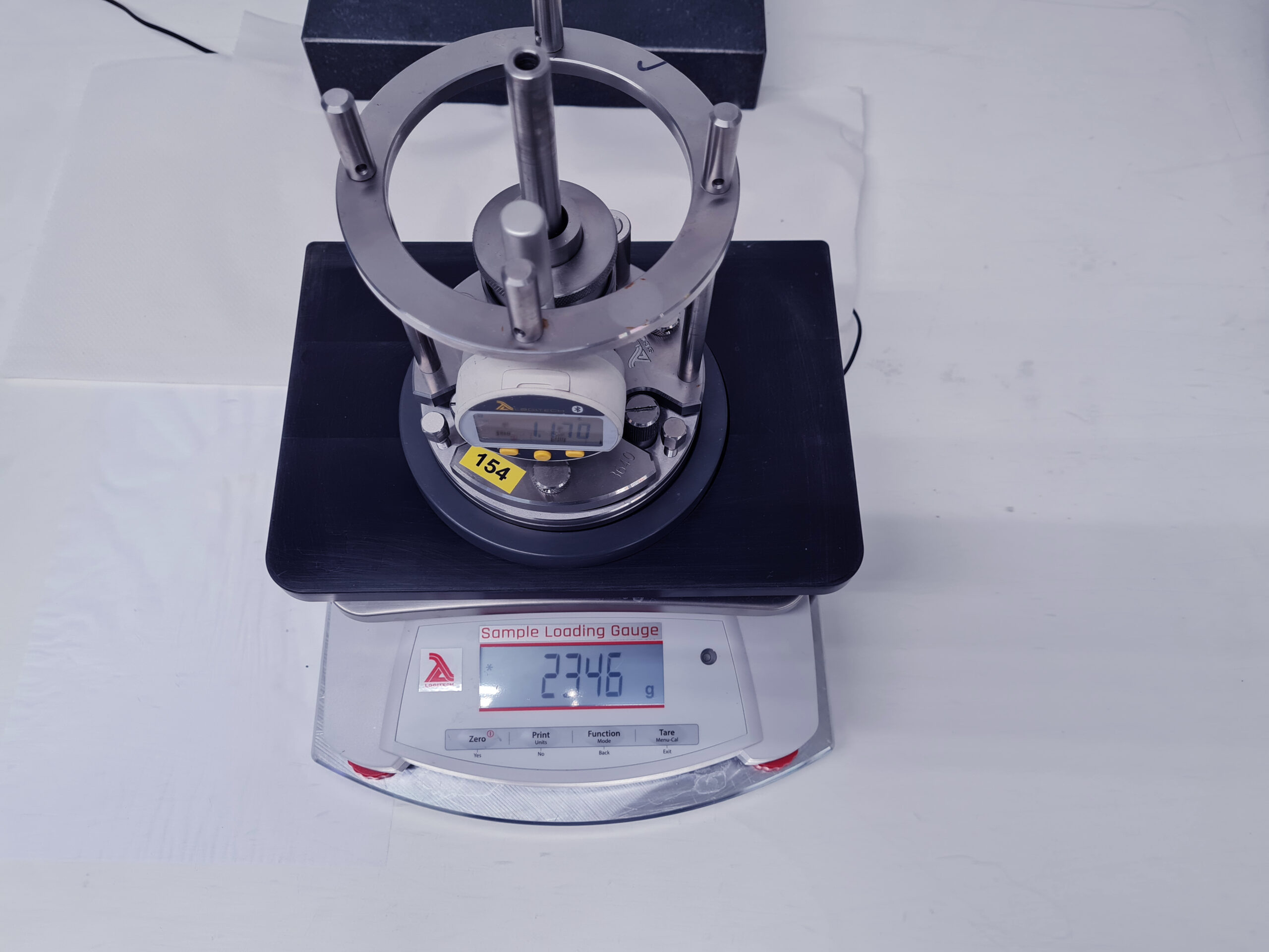
The Logitech Sample Loading Gauge provides the operator with an accurate means to measure the load exerted by a jig on a sample of up to 4″(102mm) diameter. From this automatic reading the operator can precisely set the required sample load at the optimal level for effective lapping.
The Sample Loading Gauge calculates in increments of 2g, recording accurate measurements of sample load up to 10kg. It is designed to be used in conjunction with the complete range of Logitech PP5 and PP6 Precision Lapping & Polishing Jigs.
Key Features
  • Precise measurement of sample load
  • Elimination of manual calculation
  • Highest standards of process repeatability
  • Accepts sample loads of up to 10kg
  • Compatible with Logitech PP5 and PP6 jigs

Applications

The sample loading gauge accurately measures the sample load of diverse material types.  These include semiconductor, opto-electronic and laser applications.  The adaptability of the gauge provides you with the flexibility to set very light loads of between 100g and 200g per cm².  This is extremely beneficial when determining the optimal polishing parameters of very fragile non-linear optical crystals.

Product Specification:

Height: 125mm
Length: 270mm
Depth: 280mm
Weight: 4.01kg
Power supply: Adaptor or 4xC Batteries
Maximum load: 10kg

Visit our Online Consumables store

Product Specification:

Height: 85mm
Length: 155mm
Depth: 218mm
Weight: 2.02kg
Power supply: Adaptor or 3 AA batteries
Maximum load: 5kg

Semiconductors

Semiconductor Applications

Semiconductor materials are used in a wide variety of devices such as field effect transistors (MosFets, Fets), integrated circuits (ICs, MMICs, ASICs), focal plane arrays and infra-red detectors.

Whatever the application or material, each semiconductor wafer undergoes several common stages during manufacture, which include slicing the wafer from the crystal, preparing the surface prior to fabrication and thinning the device after fabrication through the use of lapping and polishing techniques.

Logitech provide complete system solutions including consumables for the precise thinning of these III-V, I.R. and similar materials.

Optoelectronics

Logitech Optoelectronic Material Processing Systems

Advances in communication technology have led to the development of a wide variety of optoelectronics and integrated optics devices for applications such as; dense wavelength division multiplexing (DWDM), optical isolators, signal processors and optical switching.

Logitech has a large selection of adaptable systems for the preparation of optoelectronic materials such as; silicon, lithium niobate, lithium tantalate, bismuith silicon oxide, barium titanate and similar materials.

Our systems, accessories and consumables provide defect free face and edge polishing on optoelectronic substrate and scratch free surfaces with exacting and repeatable dimensional tolerances.

Optics

Systems for Optical Material Applications

The importance of optical polishing and the processing of optical components has never been greater with the ongoing development of the telecommunications market. Whether for Infra Red and polymer waveguide production or fibre optic cable polishing.

The precision design and manufacture of our equipment enable you to obtain maximum results from the cutting, lapping and polishing of these optical materials.

the-tech-files

Expert news and views to help sharpen your cutting edge

DIAMONDS ARE AN ENGINEER’S BEST FRIEND

In recent years, diamond has emerged as not only a girl’s best friend, but also as contender as an engineer’s best friend – if the technical challenges of exploiting its remarkable properties can be overcome.

LOGIN TO VIEW

THE END OF THE CHIP FOR SILICON?

Silicon-based semiconducting integrated circuits have changed the world immeasurably over the past 50 years. Today the number of silicon chips in use far outweighs the number of humans currently alive.

LOGIN TO VIEW

OPTIMAL FRICTION FOR OPTIMAL FLATNESS

The wafers used to make semiconducting chips for electronic devices all have one thing in common – they need to be smooth – super smooth. Typically, wafer flatness needs to be controlled within ±2 μm.

FREE TO VIEW
contact-us-icon
contact-us-icon
contact-us-icon

Home  |  Sitemap  |  Privacy Policy  | Cookies Policy | Environmental Policy | Contact Us  |  Extranet | Indicor

We are using cookies to give you the best experience on our website.

You can find out more about which cookies we are using or switch them off in .

Powered by  GDPR Cookie Compliance
Privacy Overview

This website uses cookies so that we can provide you with the best user experience possible. Cookie information is stored in your browser and performs functions such as recognising you when you return to our website and helping our team to understand which sections of the website you find most interesting and useful.

Strictly Necessary Cookies

Strictly Necessary Cookie should be enabled at all times so that we can save your preferences for cookie settings.

If you disable this cookie, we will not be able to save your preferences. This means that every time you visit this website you will need to enable or disable cookies again.