Extranet Login

t: +44 (0)1389 875444|e:enquiries@logitech.uk.com

  • Who we are
    • Our History
    • Quality & Accreditations
    • Our Environmental Policies
      • Our WEEE Policy
    • Careers
  • What we offer
    • By application
      • Semiconductors
      • Geological Sciences
      • Optoelectronics
      • Optics
      • Other applications
    • By material
      • Silicon
      • Silicon Carbide
      • Sapphire
      • Gallium Arsenide
      • Cadmium Zinc Telluride
      • Indium Phosphide
      • Rock/Soil
      • Other Materials
  • Products & Solutions
    • Lapping & Polishing
    • Chemical Polishing & Chemical Mechanical Polishing
    • Driven Head Lapping & Polishing Tools
    • Bonding & Impregnation Units
    • Test & Measurement
    • Cutting & Sawing
    • Accessories
    • Consumable Items
    • Consumables Store
  • Knowledge base
    • Whitepapers
    • Tech Files – Blog
    • Technology Transfer Programme
    • Brochures
    • Application Process Notes
    • Case Studies
    • FAQ
  • News & Events
    • News
    • Events
  • Contact
    • How to find us
    • Global Distributors
    • Equipment Returns
Menu
  • Who we are
    • Our History
    • Quality & Accreditations
    • Our Environmental Policies
      • Our WEEE Policy
    • Careers
  • What we offer
    • By application
      • Semiconductors
      • Geological Sciences
      • Optoelectronics
      • Optics
      • Other applications
    • By material
      • Silicon
      • Silicon Carbide
      • Sapphire
      • Gallium Arsenide
      • Cadmium Zinc Telluride
      • Indium Phosphide
      • Rock/Soil
      • Other Materials
  • Products & Solutions
    • Lapping & Polishing
    • Chemical Polishing & Chemical Mechanical Polishing
    • Driven Head Lapping & Polishing Tools
    • Bonding & Impregnation Units
    • Test & Measurement
    • Cutting & Sawing
    • Accessories
    • Consumable Items
    • Consumables Store
  • Knowledge base
    • Whitepapers
    • Tech Files – Blog
    • Technology Transfer Programme
    • Brochures
    • Application Process Notes
    • Case Studies
    • FAQ
  • News & Events
    • News
    • Events
  • Contact
    • How to find us
    • Global Distributors
    • Equipment Returns
Home  /  Chemical Polishing & Chemical Mechanical Polishing  /  CMP-Orbis Standing CMP System

CMP-Orbis Standing CMP System

Categories: Chemical Polishing & Chemical Mechanical Polishing, View All
  • Tribo CMP System
  • Tribo CMP System

Product Video:

  • Description
  • TECHNICAL SPECIFICATIONS
  • Applications
  • Case Studies
  • Accessories & Consumables

Description

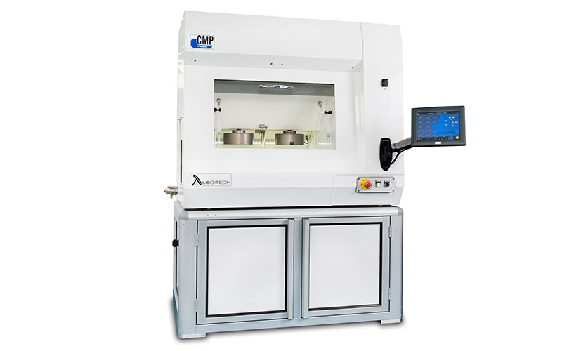
The Logitech Orbis CMP system is a precision engineered, floor standing CMP tool ideally suited for R&D environments.  Typically the Orbis CMP System is used in applications which conduct pilot production tests with optimum analytical capabilities and enhanced processing performance.

The system capabilities can be adapted to include:

  • Back-end IC manufacturing,
  • Micro-Electromechanical Systems (MEMS) fabrication,
  • Opto-MEMS
  • Bio-MEMS fabrication.

Low cost solution – high value results
The ability to conduct pilot process tests normally requires expensive production level systems, yet the Orbis achieves this capability in a cost effective system. Incorporating enhanced features and high-tech functionality, the Orbis CMP System achieves superior processing capabilities to those usually offered in a system of this size.

Flexible use of operation
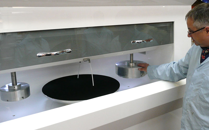
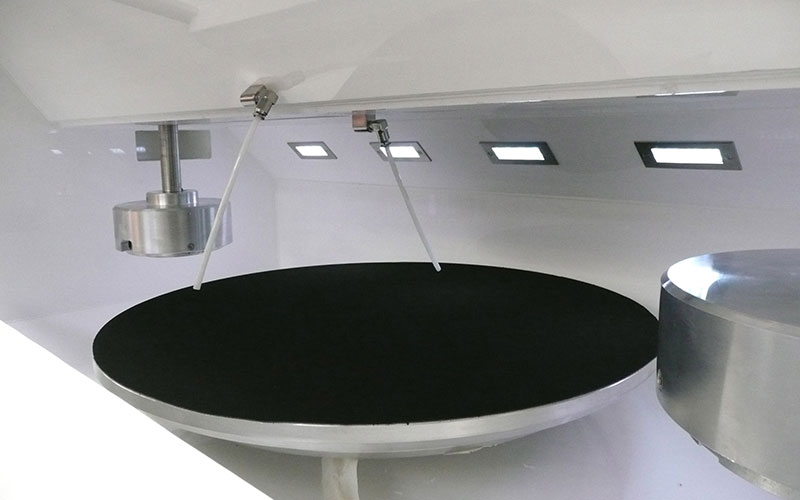
In addition to its ability to replicate production level environments, the Orbis is also suitable for more traditional R&D usage.  This includes small batch production and pilot production testing.  The system is capable of processing all die, wafer and part wafers up to 200mm (8″) diameter using a dedicated carrier. As with previous Logitech CMP equipment, templates and shims can be utilised or the samples can be mounted directly to the sample carriers.

Post CMP Cleaning
Please contact Logitech for post CMP cleaning options.

Visit our Online Consumables store

Download Brochure

Key Features

    • Ideal for R&D environments and pilot process testing
    • High capacity workspace for samples up to 2 of 200mm (8″)
    • Downloadable data for analysis of process parameters
    • Laboratory scale footprint
    • Industry standard pad conditioning to maintain optimum pad life

Product Data:

Power Supply: Single Phase, Neutral, Earth. 220v – 240v
Fuse Rating: 25A RCBO
Plate Speed: 0-160rpm
Plate Diameter: 600mm
Plate Rotation: Forward & Reverse direction settings
Carrier 1 Speed 10-125rpm
Carrier 2 Speed 10-125rpm Max
Carrier Sizes Available: 100mm (4″); 150mm (6″); 200mm(8″) wafer
Height: 1950mm
Depth: 735mm – 785mm (including front bar)
Width: 1680mm + control arm (180mm flat)
Net Weight: 590Kg
Gross Packed Weight: 830Kg
Chemical Compatability: Acidic & Alkaline CMP Slurries

Semiconductors

semiconductors

Semiconductor materials are used in a wide variety of devices such as field effect transistors (MosFets, Fets), integrated circuits (ICs, MMICs, ASICs), focal plane arrays and infra-red detectors.

Whatever the application or material, each semiconductor wafer undergoes several common stages during manufacture, which include slicing the wafer from the crystal, preparing the surface prior to fabrication and thinning the device after fabrication through the use of lapping and polishing techniques.

Logitech provide complete system solutions including consumables for the precise thinning of these III-V, I.R. and similar materials.

Optoelectronics

optoelectronics

Advances in communication technology have led to the development of a wide variety of optoelectronics and integrated optics devices for applications such as; dense wavelength division multiplexing (DWDM), optical isolators, signal processors and optical switching.

Logitech has a large selection of adaptable systems for the preparation of optoelectronic materials such as; silicon, lithium niobate, lithium tantalate, bismuith silicon oxide, barium titanate and similar materials.

Our systems, accessories and consumables provide defect free face and edge polishing on optoelectronic substrate and scratch free surfaces with exacting and repeatable dimensional tolerances.

Optics

optics

The importance of optical polishing and the processing of optical components has never been greater with the ongoing development of the telecommunications market. Whether for Infra Red and polymer waveguide production or fibre optic cable polishing.

The precision design and manufacture of our equipment enable you to obtain maximum results from the cutting, lapping and polishing of these optical materials.

CMP Applications

Primary applications areas are in the field of Tribology Science and Research, particularly with regards process and analysis results.  For example co-efficient of friction monitoring (CoF).

The Tribo chemical mechanical polishing system is also readily adaptable as an enabling technology in Microelectromechanical Systems (MEMS) fabrication, particularly polysilicon surface micromachining, Opto-MEMS and Bio-MEMS packaging, assembly and even fabrication.


Polishing Plates

polishingplates

The Logitech range of polishing plates provides a comprehensive selection for polishing a wide range of materials.

Chemcloth Polishing Cloths

Logitech Chemcloth Polishing Cloths are designed to meet the needs of today’s (Chemical Mechanical Polishing (CMP) operations.

EP Polishing Pads and Cloths

Logitech EP1 and EP2 Chemical Mechanical Polishing (CMP) Polishing Cloths and pads are suitable for a wide range of applications.  Including oxide, nitride and copper.

Polishing Suspensions

Logitech polishing suspensions have been developed to suit a wide range of polishing applications in the semiconductor and optoelectronics industries.

Standard Templates


the-tech-files

Expert news and views to help sharpen your cutting edge

DIAMONDS ARE AN ENGINEER’S BEST FRIEND

In recent years, diamond has emerged as not only a girl’s best friend, but also as contender as an engineer’s best friend – if the technical challenges of exploiting its remarkable properties can be overcome.

LOGIN TO VIEW

THE END OF THE CHIP FOR SILICON?

Silicon-based semiconducting integrated circuits have changed the world immeasurably over the past 50 years. Today the number of silicon chips in use far outweighs the number of humans currently alive.

LOGIN TO VIEW

OPTIMAL FRICTION FOR OPTIMAL FLATNESS

The wafers used to make semiconducting chips for electronic devices all have one thing in common – they need to be smooth – super smooth. Typically, wafer flatness needs to be controlled within ±2 μm.

FREE TO VIEW
contact-us-icon
contact-us-icon
contact-us-icon

Home  |  Sitemap  |  Privacy Policy  | Cookies Policy | Environmental Policy | Contact Us  |  Extranet | Indicor

We are using cookies to give you the best experience on our website.

You can find out more about which cookies we are using or switch them off in .

Powered by  GDPR Cookie Compliance
Privacy Overview

This website uses cookies so that we can provide you with the best user experience possible. Cookie information is stored in your browser and performs functions such as recognising you when you return to our website and helping our team to understand which sections of the website you find most interesting and useful.

Strictly Necessary Cookies

Strictly Necessary Cookie should be enabled at all times so that we can save your preferences for cookie settings.

If you disable this cookie, we will not be able to save your preferences. This means that every time you visit this website you will need to enable or disable cookies again.