Extranet Login

t: +44 (0)1389 875444|e:enquiries@logitech.uk.com

  • Who we are
    • Our History
    • Quality & Accreditations
    • Our Environmental Policies
      • Our WEEE Policy
    • Careers
  • What we offer
    • By application
      • Semiconductors
      • Geological Sciences
      • Optoelectronics
      • Optics
      • Other applications
    • By material
      • Silicon
      • Silicon Carbide
      • Sapphire
      • Gallium Arsenide
      • Cadmium Zinc Telluride
      • Indium Phosphide
      • Rock/Soil
      • Other Materials
  • Products & Solutions
    • Lapping & Polishing
    • Chemical Polishing & Chemical Mechanical Polishing
    • Driven Head Lapping & Polishing Tools
    • Bonding & Impregnation Units
    • Test & Measurement
    • Cutting & Sawing
    • Accessories
    • Consumable Items
    • Consumables Store
  • Knowledge base
    • Whitepapers
    • Tech Files – Blog
    • Technology Transfer Programme
    • Brochures
    • Application Process Notes
    • Case Studies
    • FAQ
  • News & Events
    • News
    • Events
  • Contact
    • How to find us
    • Global Distributors
    • Equipment Returns
Menu
  • Who we are
    • Our History
    • Quality & Accreditations
    • Our Environmental Policies
      • Our WEEE Policy
    • Careers
  • What we offer
    • By application
      • Semiconductors
      • Geological Sciences
      • Optoelectronics
      • Optics
      • Other applications
    • By material
      • Silicon
      • Silicon Carbide
      • Sapphire
      • Gallium Arsenide
      • Cadmium Zinc Telluride
      • Indium Phosphide
      • Rock/Soil
      • Other Materials
  • Products & Solutions
    • Lapping & Polishing
    • Chemical Polishing & Chemical Mechanical Polishing
    • Driven Head Lapping & Polishing Tools
    • Bonding & Impregnation Units
    • Test & Measurement
    • Cutting & Sawing
    • Accessories
    • Consumable Items
    • Consumables Store
  • Knowledge base
    • Whitepapers
    • Tech Files – Blog
    • Technology Transfer Programme
    • Brochures
    • Application Process Notes
    • Case Studies
    • FAQ
  • News & Events
    • News
    • Events
  • Contact
    • How to find us
    • Global Distributors
    • Equipment Returns
Home  /  Bonding & Impregnation Units  /  Modular Wafer Substrate Bonder

Modular Wafer Substrate Bonder

Categories: Bonding & Impregnation Units, View All

Product Video:

  • Description
  • Facilities Requirement
  • Applications
  • Accessories & Consumables

Description

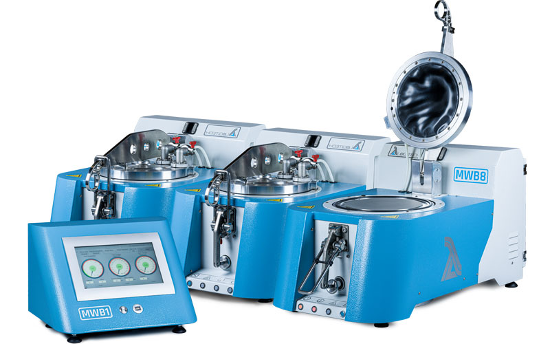
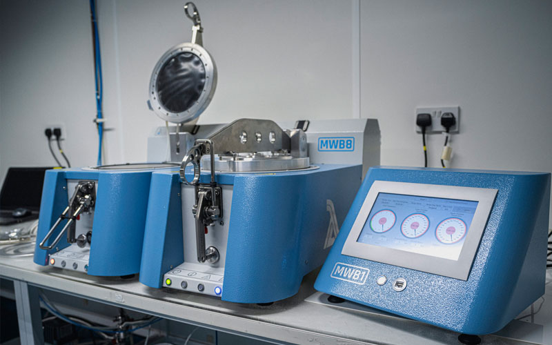
The most recent addition to our range of premium wafer bonders, the Modular Wafer Bonding System (MWBS). The MWBS offers a bonding capacity ,of small pieces of wafers and wafer sizes, from 2″ up to 8″. The modular design allows for up to 12 heads (with the capacity for expansion) from one single control unit. This saves valuable bench space and allows for easy, synchronous and asynchronous processing.


Due to the fully expandable modular design of the system, it is ideal for both R&D and production level facilities. Allowing a cost effective solution, the system is fully tailored to the exact bonding and throughput requirements of the customer.

Download Brochure

Key Features

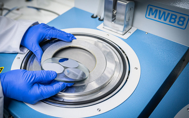
  • Wafer process capacity of small wafer pieces and wafer sizes from 2″ up to 8″ per bonding head.
  • Modular design with expansion capacity allowing a cost effective solution tailored to your exact bonding requirements.
  • Control up to 12 bonding heads (with the capacity for expansion) from a single control unit, saving valuable bench space and allowing for easy synchronous and asynchronous processing.
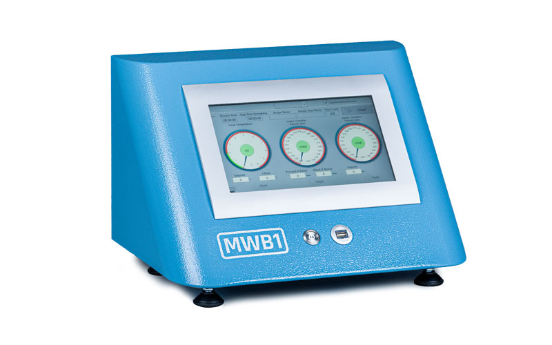
  • Easy to use fully customised recipe controlled process cycles, process conditions set via graphical user interface including bonding temperature of up to 240°C and required vacuum.

Product Specifications:

1MWB1 Control Unit 1MWB8 Bonding Head
Power Supply: Single Phase, Earth. 110-240V 0.8A

(24V DC 1.25A Input cable)

Single Phase, Earth. 240V
Height:  270mm   405mm
Depth:  285mm  700mm
Width: 395mm  410mm
Weight: 7kg  60kg

Semiconductors

semiconductors

Semiconductor materials are used in a wide variety of devices such as field effect transistors (MosFets, Fets), integrated circuits (ICs, MMICs, ASICs), focal plane arrays and infra-red detectors.

Whatever the application or material, each semiconductor wafer undergoes several common stages during manufacture, which include slicing the wafer from the crystal, preparing the surface prior to fabrication and thinning the device after fabrication through the use of lapping and polishing techniques.

Logitech provide complete system solutions including consumables for the precise thinning of these III-V, I.R. and similar materials.

Optoelectronics

optoelectronics

Advances in communication technology have led to the development of a wide variety of optoelectronics and integrated optics devices for applications such as; dense wavelength division multiplexing (DWDM), optical isolators, signal processors and optical switching.

Logitech has a large selection of adaptable systems for the preparation of optoelectronic materials such as; silicon, lithium niobate, lithium tantalate, bismuith silicon oxide, barium titanate and similar materials.

Our systems, accessories and consumables provide defect free face and edge polishing on optoelectronic substrate and scratch free surfaces with exacting and repeatable dimensional tolerances.

Optics

optics

The importance of optical polishing and the processing of optical components has never been greater with the ongoing development of the telecommunications market. Whether for Infra Red and polymer waveguide production or fibre optic cable polishing.

The precision design and manufacture of our equipment enable you to obtain maximum results from the cutting, lapping and polishing of these optical materials.

Mounting Adhesives

Logitech provides a range of mounting media for bonding of semiconductor, optic and geological samples.

Glass Microscope Slides

Logitech glass microscope slides are used for the permanent mounting of thin rock, concrete and soil thin sections.

Glass Slide Coverslips

Glass coverslips protect valuable thin sections and improve optical clarity for transmitted microscopy.

the-tech-files

Expert news and views to help sharpen your cutting edge

DIAMONDS ARE AN ENGINEER’S BEST FRIEND

In recent years, diamond has emerged as not only a girl’s best friend, but also as contender as an engineer’s best friend – if the technical challenges of exploiting its remarkable properties can be overcome.

LOGIN TO VIEW

THE END OF THE CHIP FOR SILICON?

Silicon-based semiconducting integrated circuits have changed the world immeasurably over the past 50 years. Today the number of silicon chips in use far outweighs the number of humans currently alive.

LOGIN TO VIEW

OPTIMAL FRICTION FOR OPTIMAL FLATNESS

The wafers used to make semiconducting chips for electronic devices all have one thing in common – they need to be smooth – super smooth. Typically, wafer flatness needs to be controlled within ±2 μm.

FREE TO VIEW
contact-us-icon
contact-us-icon
contact-us-icon

Home  |  Sitemap  |  Privacy Policy  | Cookies Policy | Environmental Policy | Contact Us  |  Extranet | Indicor

We are using cookies to give you the best experience on our website.

You can find out more about which cookies we are using or switch them off in .

Powered by  GDPR Cookie Compliance
Privacy Overview

This website uses cookies so that we can provide you with the best user experience possible. Cookie information is stored in your browser and performs functions such as recognising you when you return to our website and helping our team to understand which sections of the website you find most interesting and useful.

Strictly Necessary Cookies

Strictly Necessary Cookie should be enabled at all times so that we can save your preferences for cookie settings.

If you disable this cookie, we will not be able to save your preferences. This means that every time you visit this website you will need to enable or disable cookies again.