Extranet Login

t: +44 (0)1389 875444|e:enquiries@logitech.uk.com

  • Who we are
    • Our History
    • Quality & Accreditations
    • Our Environmental Policies
      • Our WEEE Policy
    • Careers
  • What we offer
    • By application
      • Semiconductors
      • Geological Sciences
      • Optoelectronics
      • Optics
      • Other applications
    • By material
      • Silicon
      • Silicon Carbide
      • Sapphire
      • Gallium Arsenide
      • Cadmium Zinc Telluride
      • Indium Phosphide
      • Rock/Soil
      • Other Materials
  • Products & Solutions
    • Lapping & Polishing
    • Chemical Polishing & Chemical Mechanical Polishing
    • Driven Head Lapping & Polishing Tools
    • Bonding & Impregnation Units
    • Test & Measurement
    • Cutting & Sawing
    • Accessories
    • Consumable Items
    • Consumables Store
  • Knowledge base
    • Whitepapers
    • Tech Files – Blog
    • Technology Transfer Programme
    • Brochures
    • Application Process Notes
    • Case Studies
    • FAQ
  • News & Events
    • News
    • Events
  • Contact
    • How to find us
    • Global Distributors
    • Equipment Returns
Menu
  • Who we are
    • Our History
    • Quality & Accreditations
    • Our Environmental Policies
      • Our WEEE Policy
    • Careers
  • What we offer
    • By application
      • Semiconductors
      • Geological Sciences
      • Optoelectronics
      • Optics
      • Other applications
    • By material
      • Silicon
      • Silicon Carbide
      • Sapphire
      • Gallium Arsenide
      • Cadmium Zinc Telluride
      • Indium Phosphide
      • Rock/Soil
      • Other Materials
  • Products & Solutions
    • Lapping & Polishing
    • Chemical Polishing & Chemical Mechanical Polishing
    • Driven Head Lapping & Polishing Tools
    • Bonding & Impregnation Units
    • Test & Measurement
    • Cutting & Sawing
    • Accessories
    • Consumable Items
    • Consumables Store
  • Knowledge base
    • Whitepapers
    • Tech Files – Blog
    • Technology Transfer Programme
    • Brochures
    • Application Process Notes
    • Case Studies
    • FAQ
  • News & Events
    • News
    • Events
  • Contact
    • How to find us
    • Global Distributors
    • Equipment Returns
Home  /  Cutting & Sawing  /  GTS1 Thin Section Cut-Off and Trim Saw

GTS1 Thin Section Cut-Off and Trim Saw

Categories: Cutting & Sawing, View All
  • GTS1 Thin Section Saw
  • GS1 Thin Section Saw
  • GTS1 Thin Section Saw
  • GS1 Thin Section Saw
  • Description
  • Facilities Requirement
  • Applications
  • Accessories & Consumables

Description

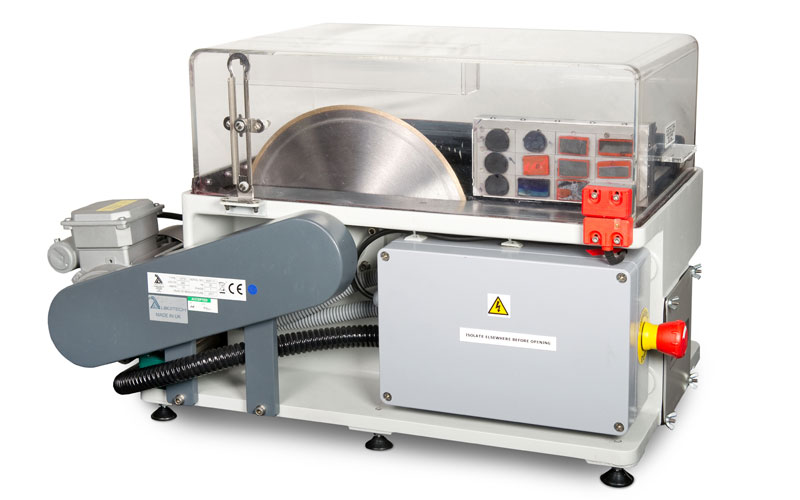
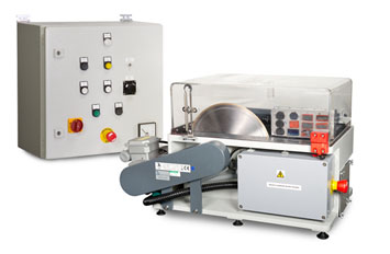
The GTS1 Thin Section Cut-Off and Trim Saw is a compact, bench-top unit for the preparation of geological thin sections.  The saw is ideal for cutting bulk rocks and thinning mounted sections of rock.

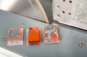
When cutting the mounted rock, there are two main considerations:

  • The thinned rock sample should be as thin as possible, in order to reduce the subsequent lapping time
  • The cut should be of the highest possible quality, to ensure that sub-surface damage is kept to a minimum.

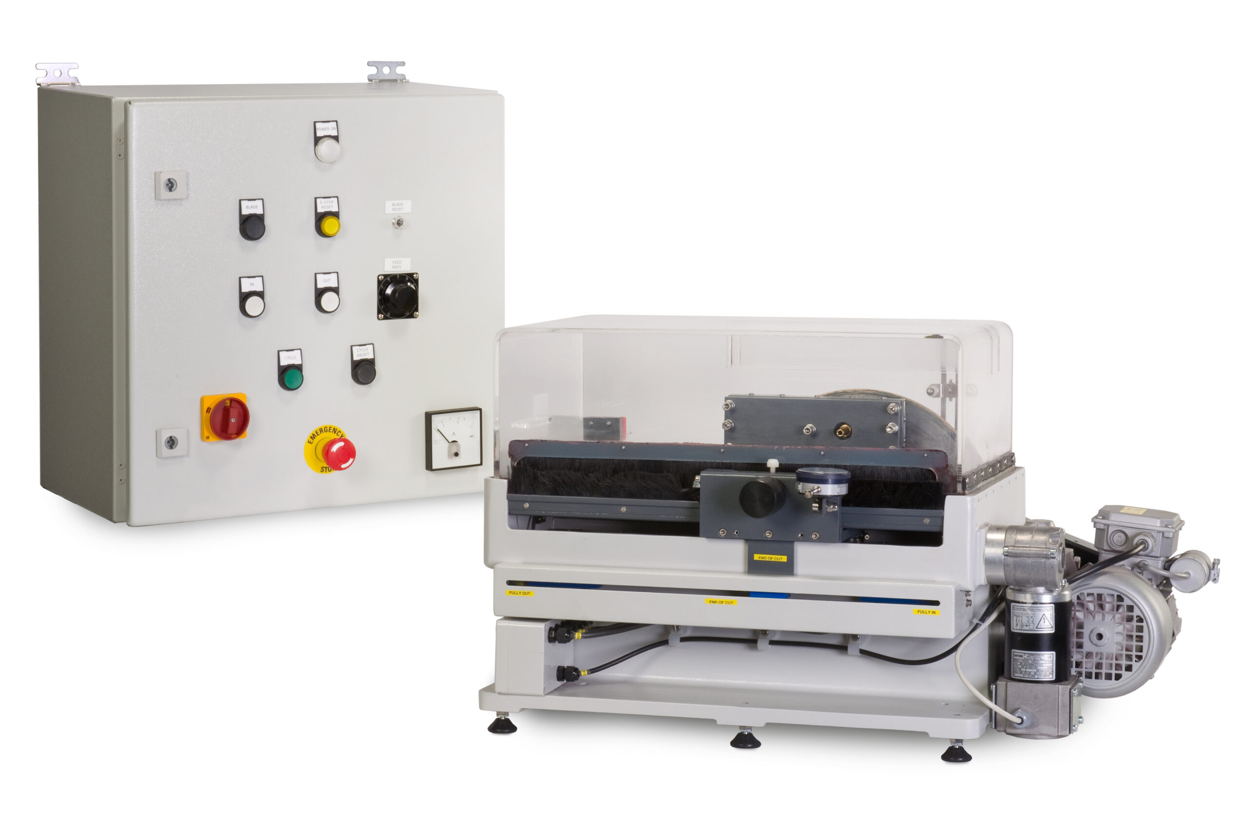
The GTS1 Thin Section Cut-Off and Trim Saw offers a number of advantages over other saws.  In particular, the variable speed linear drive system and feed rate monitor allow the operator to control the rate at which the samples move through the blade. This avoids many of the problems associated with gravity-fed systems, such as slides shattering if the entire cutting force is exerted on a small part of the sample at the end of the cutting operation.

For vacuum mounting of samples the VS2 Vacuum system is an ideal fit with GTS1 saw.

Visit our Online Consumables store

Download Brochure

Key Features

  • Pre-thinning of slides to selected thickness
  • Accepts multiple slides up to 12 of 28mm x 48mm
  • Automatic operating cycle
  • Excellent cut quality and uniformity to 200 microns

Product Specification:

Power Supply: 220/240V, 50-60Hz or 110V, 50/60Hz
Main Drive Motor: 0.55kW
Height: 510mm
Width: 400mm
Depth: 720mm
Diamond Blade: 300mm diameter x 2.0mm thick
Standard Slide Capacities: 12 of 28mm x 48mm
 7 of 25mm x 76mm
 3 of 50mm x 76mm
 1 of 110mm x 76mm
Weight: 60kg

Geological Sciences

geologicalsciences

In many areas of geological study such as mineralogy, petrography and sedimentology you are required to analyse the characteristics of the materials such as soil or rock.  To be able to do this a thin section needs to be prepared for microscopic examination.

Logitech precision equipment is ideal for thin or ultra-thin section preparation.  Our wide range of versatile systems enable you to trim, lap and polish geological thin sections such as rock, coal, concete and soils.

Each of our systems are fully supported by a wide range of accessories and consumables, such as abrasive powders, polishing cloths and mounting media.

VS2

vs2

The versatile VS2 unit provides a ‘ready to use’ system for vacuum retention of samples on a variety of lapping and polishing jigs and machines.

Saw Blades & Cutting Wires

High quality diamond and silicon carbide saw blades and a selection of steel and diamond cutting wire to fit all Logitech saws.

Carrier Disc & Substrates

Logitech glass carrier discs are used for the temporary support of both semiconductor and opto-electronics wafers during thinning and polishing operations.

Mounting Adhesives

Logitech provides a range of mounting media for bonding of semiconductor, optic and geological samples.

the-tech-files

Expert news and views to help sharpen your cutting edge

DIAMONDS ARE AN ENGINEER’S BEST FRIEND

In recent years, diamond has emerged as not only a girl’s best friend, but also as contender as an engineer’s best friend – if the technical challenges of exploiting its remarkable properties can be overcome.

LOGIN TO VIEW

THE END OF THE CHIP FOR SILICON?

Silicon-based semiconducting integrated circuits have changed the world immeasurably over the past 50 years. Today the number of silicon chips in use far outweighs the number of humans currently alive.

LOGIN TO VIEW

OPTIMAL FRICTION FOR OPTIMAL FLATNESS

The wafers used to make semiconducting chips for electronic devices all have one thing in common – they need to be smooth – super smooth. Typically, wafer flatness needs to be controlled within ±2 μm.

FREE TO VIEW
contact-us-icon
contact-us-icon
contact-us-icon

Home  |  Sitemap  |  Privacy Policy  | Cookies Policy | Environmental Policy | Contact Us  |  Extranet | Indicor

We are using cookies to give you the best experience on our website.

You can find out more about which cookies we are using or switch them off in .

Powered by  GDPR Cookie Compliance
Privacy Overview

This website uses cookies so that we can provide you with the best user experience possible. Cookie information is stored in your browser and performs functions such as recognising you when you return to our website and helping our team to understand which sections of the website you find most interesting and useful.

Strictly Necessary Cookies

Strictly Necessary Cookie should be enabled at all times so that we can save your preferences for cookie settings.

If you disable this cookie, we will not be able to save your preferences. This means that every time you visit this website you will need to enable or disable cookies again.