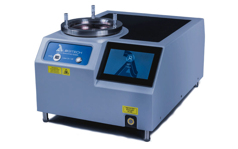
Extranet Login

t: +44 (0)1389 875444|e:enquiries@logitech.uk.com

  • Who we are
    • Our History
    • Quality & Accreditations
    • Our Environmental Policies
      • Our WEEE Policy
    • Careers
  • What we offer
    • By application
      • Semiconductors
      • Geological Sciences
      • Optoelectronics
      • Optics
      • Other applications
    • By material
      • Silicon
      • Silicon Carbide
      • Sapphire
      • Gallium Arsenide
      • Cadmium Zinc Telluride
      • Indium Phosphide
      • Rock/Soil
      • Other Materials
  • Products & Solutions
    • Lapping & Polishing
    • Chemical Polishing & Chemical Mechanical Polishing
    • Driven Head Lapping & Polishing Tools
    • Bonding & Impregnation Units
    • Test & Measurement
    • Cutting & Sawing
    • Accessories
    • Consumable Items
    • Consumables Store
  • Knowledge base
    • Whitepapers
    • Tech Files – Blog
    • Technology Transfer Programme
    • Brochures
    • Application Process Notes
    • Case Studies
    • FAQ
  • News & Events
    • News
    • Events
  • Contact
    • How to find us
    • Global Distributors
    • Equipment Returns
Menu
  • Who we are
    • Our History
    • Quality & Accreditations
    • Our Environmental Policies
      • Our WEEE Policy
    • Careers
  • What we offer
    • By application
      • Semiconductors
      • Geological Sciences
      • Optoelectronics
      • Optics
      • Other applications
    • By material
      • Silicon
      • Silicon Carbide
      • Sapphire
      • Gallium Arsenide
      • Cadmium Zinc Telluride
      • Indium Phosphide
      • Rock/Soil
      • Other Materials
  • Products & Solutions
    • Lapping & Polishing
    • Chemical Polishing & Chemical Mechanical Polishing
    • Driven Head Lapping & Polishing Tools
    • Bonding & Impregnation Units
    • Test & Measurement
    • Cutting & Sawing
    • Accessories
    • Consumable Items
    • Consumables Store
  • Knowledge base
    • Whitepapers
    • Tech Files – Blog
    • Technology Transfer Programme
    • Brochures
    • Application Process Notes
    • Case Studies
    • FAQ
  • News & Events
    • News
    • Events
  • Contact
    • How to find us
    • Global Distributors
    • Equipment Returns
Home  /  Test & Measurement  /  GI20 Flatness Measurement

GI20 Flatness Measurement

Categories: Test & Measurement, View All
  • GI Flatness Measurement
  • Description
  • Facilities Requirement
  • Applications

Description


Logitech’s GI20 Flatness Measurement instrument provides high precision flatness measurement suitable for use with lapped and semi-polished surfaces up to 150mm (6″)Ø. Unlike conventional fizeau interferometers, the GI20 can be used for measuring non-reflective surfaces, making it ideal for carrying out checks on lapped and/or ground surfaces prior to final polishing.

The interferogram is displayed on a screen at the front of the unit. A parallel display can be created via the HDMI port and images can also be exported through the USB port for external analysis. All features of the interferometer are controlled via the touch screen panel.

Grazing Incidence Interferometry
A standard fizeau interferometer will, depending on the wavelength used, normally operate with fringe spacing approximately 0.3µm. This often restricts flatness measurements to highly reflective materials which will provide sufficient contrast on the monitor. The resulting short distances between fringes often impedes the analysis of “busy” images.

Logitech Grazing Incidence Interferometers overcome such problems by reflection of laser light at a grazing incidence angle off the sample surface. This angled beam of light ensures that the monitor shows fringes on both reflective and non-reflective sample surfaces. It also allows a large visible aperture of 127mm x 150mm (5″ x 6″), enabling samples of up to 150mm (6″)Ø to be accurately assessed.

The 7″ screen allows rapid and accurate measurements to be made “in process” with fringe spacing displayed at a fixed 2µm interval, producing excellent contrast levels with surface finishes from polished samples up to 300nm Ra. Evaluation of fringe patterns can be done  by exporting images via USB port.

Applications:
Applications for the GI20 Flatness Measurement System is virtually limitless. Whether the requirement is for flatness measurement or quality assessment, the Logitech Grazing Incidence Interferometer provides an excellent solution when processing semiconductor wafers; optical components; machined components and geological samples.

Manual Grazing Incidence Interferometry:
Each fringe shown on the screen represents a 2mm change in the air gap between the specimen and the reference. Convexity and concavity are determined by gentle finger pressure as if to close the air gap.

Fringes move away from the point of the air gap (i.e. area of roundness) and conversely towards the maximum air gap (i.e. area of hollowness). As interferometry determines any departure from specimen flatness and requires some degree of tilt between the specimen and the reference flat, it is necessary to compensate for any residual net tilt by visually minimising the fringe count.

Product Specification:

Power supply: 240V/110V, 50Hz
Height: 260mm
Depth: 602mm
Width: 430mm
Weight: 24kg
Maximum sample size:            150mm (6″)
Surface roughness: 1nm to 300nm Ra
Fringe spacing: 2µm

Visit our Online Consumables store

Download Brochure

Key Features

  • High precision flatness measurement of ground, lapped or semi-polished samples
  • Measure 2µm per fringe with excellent clarity
  • Surface roughness measurement from 1nm to 300nm Ra

Product Specification:

Power supply: 240V/110V, 50Hz
Height: 260mm
Depth: 602mm
Width: 430mm
Weight: 24kg
Maximum sample size:            150mm (6″)
Surface roughness: 1nm to 300nm Ra
Fringe spacing: 2µm

Optoelectronics

optoelectronics

Advances in communication technology have led to the development of a wide variety of optoelectronics and integrated optics devices for applications such as; dense wavelength division multiplexing (DWDM), optical isolators, signal processors and optical switching.

Logitech has a large selection of adaptable systems for the preparation of optoelectronic materials such as; silicon, lithium niobate, lithium tantalate, bismuith silicon oxide, barium titanate and similar materials.

Our systems, accessories and consumables provide defect free face and edge polishing on optoelectronic substrate and scratch free surfaces with exacting and repeatable dimensional tolerances.

Optics

optics

The importance of optical polishing and the processing of optical components has never been greater with the ongoing development of the telecommunications market. Whether for Infra Red and polymer waveguide production or fibre optic cable polishing.

The precision design and manufacture of our equipment enable you to obtain maximum results from the cutting, lapping and polishing of these optical materials.

Other Applications

otherapplications

Logitech systems are used by organisations across the world for many different complex sample preparation processes.

Including the thin section preparation of; Teeth, Bone, Otoliths, Ceramics, Metals, Alloys, Polymers and other Carbon-based materials.

Semiconductors

semiconductors

Semiconductor materials are used in a wide variety of devices such as field effect transistors (MosFets, Fets), integrated circuits (ICs, MMICs, ASICs), focal plane arrays and infra-red detectors.

Whatever the application or material, each semiconductor wafer undergoes several common stages during manufacture, which include slicing the wafer from the crystal, preparing the surface prior to fabrication and thinning the device after fabrication through the use of lapping and polishing techniques.

Logitech provide complete system solutions including consumables for the precise thinning of these III-V, I.R. and similar materials.

the-tech-files

Expert news and views to help sharpen your cutting edge

DIAMONDS ARE AN ENGINEER’S BEST FRIEND

In recent years, diamond has emerged as not only a girl’s best friend, but also as contender as an engineer’s best friend – if the technical challenges of exploiting its remarkable properties can be overcome.

LOGIN TO VIEW

THE END OF THE CHIP FOR SILICON?

Silicon-based semiconducting integrated circuits have changed the world immeasurably over the past 50 years. Today the number of silicon chips in use far outweighs the number of humans currently alive.

LOGIN TO VIEW

OPTIMAL FRICTION FOR OPTIMAL FLATNESS

The wafers used to make semiconducting chips for electronic devices all have one thing in common – they need to be smooth – super smooth. Typically, wafer flatness needs to be controlled within ±2 μm.

FREE TO VIEW
contact-us-icon
contact-us-icon
contact-us-icon

Home  |  Sitemap  |  Privacy Policy  | Cookies Policy | Environmental Policy | Contact Us  |  Extranet | Indicor

We are using cookies to give you the best experience on our website.

You can find out more about which cookies we are using or switch them off in .

Powered by  GDPR Cookie Compliance
Privacy Overview

This website uses cookies so that we can provide you with the best user experience possible. Cookie information is stored in your browser and performs functions such as recognising you when you return to our website and helping our team to understand which sections of the website you find most interesting and useful.

Strictly Necessary Cookies

Strictly Necessary Cookie should be enabled at all times so that we can save your preferences for cookie settings.

If you disable this cookie, we will not be able to save your preferences. This means that every time you visit this website you will need to enable or disable cookies again.