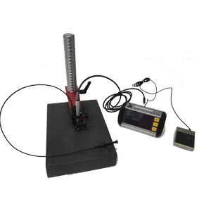
Extranet Login

t: +44 (0)1389 875444|e:enquiries@logitech.uk.com

  • Who we are
    • Our History
    • Quality & Accreditations
    • Our Environmental Policies
      • Our WEEE Policy
    • Careers
  • What we offer
    • By application
      • Semiconductors
      • Geological Sciences
      • Optoelectronics
      • Optics
      • Other applications
    • By material
      • Silicon
      • Silicon Carbide
      • Sapphire
      • Gallium Arsenide
      • Cadmium Zinc Telluride
      • Indium Phosphide
      • Rock/Soil
      • Other Materials
  • Products & Solutions
    • Lapping & Polishing
    • Chemical Polishing & Chemical Mechanical Polishing
    • Driven Head Lapping & Polishing Tools
    • Bonding & Impregnation Units
    • Test & Measurement
    • Cutting & Sawing
    • Accessories
    • Consumable Items
    • Consumables Store
  • Knowledge base
    • Whitepapers
    • Tech Files – Blog
    • Technology Transfer Programme
    • Brochures
    • Application Process Notes
    • Case Studies
    • FAQ
  • News & Events
    • News
    • Events
  • Contact
    • How to find us
    • Global Distributors
    • Equipment Returns
Menu
  • Who we are
    • Our History
    • Quality & Accreditations
    • Our Environmental Policies
      • Our WEEE Policy
    • Careers
  • What we offer
    • By application
      • Semiconductors
      • Geological Sciences
      • Optoelectronics
      • Optics
      • Other applications
    • By material
      • Silicon
      • Silicon Carbide
      • Sapphire
      • Gallium Arsenide
      • Cadmium Zinc Telluride
      • Indium Phosphide
      • Rock/Soil
      • Other Materials
  • Products & Solutions
    • Lapping & Polishing
    • Chemical Polishing & Chemical Mechanical Polishing
    • Driven Head Lapping & Polishing Tools
    • Bonding & Impregnation Units
    • Test & Measurement
    • Cutting & Sawing
    • Accessories
    • Consumable Items
    • Consumables Store
  • Knowledge base
    • Whitepapers
    • Tech Files – Blog
    • Technology Transfer Programme
    • Brochures
    • Application Process Notes
    • Case Studies
    • FAQ
  • News & Events
    • News
    • Events
  • Contact
    • How to find us
    • Global Distributors
    • Equipment Returns
Home  /  Test & Measurement  /  CG10 Contact Measurement Gauge

CG10 Contact Measurement Gauge

Categories: Test & Measurement, View All
  • CG10 Contact Gauge
  • Description
  • Facilities Requirement
  • Applications

Description

The new and improved Logitech Contact Measurement Gauge (CG10) is a compact, bluetooth enabled, gauging instrument for linear dimensional measurement applications.  It offers a high degree of accuracy over a wide measuring range with low gauging forces.

This simple to operate digital system gives an accuracy of 1µm over its 10mm measuring range.

The Contact Measurement Gauge can be connected to a PC where data can be recorded for external analysis and the software provided allows for seamless integration between a PC and the contact gauge. Data can be transferred via a RS232 cable with software or transferred directly via Bluetooth.This allows the user to work without the hassle of cables connecting to laptop or lab PC.

The Probe
Linear measuring range: 10mm
Accuracy over full range: 1µm
Repeatability: 0.2µm
Resolution: 0.1µm
Gauging force: 0.6 – 0.9N (0.135 – 0.203 lbf)
Zero drift: 0.1µm/°C
 
The Probe Stand
Table area: 280mm x 160mm (11″ x 6.3″)
Vertical adjustment: 150mm (5.91″)

Visit our Online Consumables store

Download Brochure

Key Features

  • Low gauging forces
  • Hand or foot operated
  • Metric measurement display
  • Accommodates samples up to 150 x 150mm
  • Accurate to ±0.001mm over 10mm
  • Bluetooth connectivity for easy data transfer or via wired RS232-to-USB comms port and provided software
The Probe
Linear measuring range: 10mm (0.4″)
Accuracy over full range: 1µm (0.0004″)
Repeatability: 0.2µm
Resolution: 0.1µm
Gauging force: 0.6 – 0.9N (0.135 – 0.203 lbf)
Zero drift: 0.1µm/°C
 
The Probe Stand
Table area: 280mm x 160mm (11″ x 6.3″)
Vertical adjustment: 150mm (5.91″)
 
The Electronic Processing Unit
Range: 50mm (1.97mm)
Resolution: 0.0001mm (0.000004″)
Power: 220V/50Hz or 110V/50-60Hz
Dimensions: 250mm x 160mm x 250mm
Net Weight: 19kg
Packed Weight: 42kg approx.

Optoelectronics

optoelectronics

Advances in communication technology have led to the development of a wide variety of optoelectronics and integrated optics devices for applications such as; dense wavelength division multiplexing (DWDM), optical isolators, signal processors and optical switching.

Logitech has a large selection of adaptable systems for the preparation of optoelectronic materials such as; silicon, lithium niobate, lithium tantalate, bismuith silicon oxide, barium titanate and similar materials.

Our systems, accessories and consumables provide defect free face and edge polishing on optoelectronic substrate and scratch free surfaces with exacting and repeatable dimensional tolerances.

Optics

optics

The importance of optical polishing and the processing of optical components has never been greater with the ongoing development of the telecommunications market. Whether for Infra Red and polymer waveguide production or fibre optic cable polishing.

The precision design and manufacture of our equipment enable you to obtain maximum results from the cutting, lapping and polishing of these optical materials.

the-tech-files

Expert news and views to help sharpen your cutting edge

DIAMONDS ARE AN ENGINEER’S BEST FRIEND

In recent years, diamond has emerged as not only a girl’s best friend, but also as contender as an engineer’s best friend – if the technical challenges of exploiting its remarkable properties can be overcome.

LOGIN TO VIEW

THE END OF THE CHIP FOR SILICON?

Silicon-based semiconducting integrated circuits have changed the world immeasurably over the past 50 years. Today the number of silicon chips in use far outweighs the number of humans currently alive.

LOGIN TO VIEW

OPTIMAL FRICTION FOR OPTIMAL FLATNESS

The wafers used to make semiconducting chips for electronic devices all have one thing in common – they need to be smooth – super smooth. Typically, wafer flatness needs to be controlled within ±2 μm.

FREE TO VIEW
contact-us-icon
contact-us-icon
contact-us-icon

Home  |  Sitemap  |  Privacy Policy  | Cookies Policy | Environmental Policy | Contact Us  |  Extranet | Indicor

We are using cookies to give you the best experience on our website.

You can find out more about which cookies we are using or switch them off in .

Powered by  GDPR Cookie Compliance
Privacy Overview

This website uses cookies so that we can provide you with the best user experience possible. Cookie information is stored in your browser and performs functions such as recognising you when you return to our website and helping our team to understand which sections of the website you find most interesting and useful.

Strictly Necessary Cookies

Strictly Necessary Cookie should be enabled at all times so that we can save your preferences for cookie settings.

If you disable this cookie, we will not be able to save your preferences. This means that every time you visit this website you will need to enable or disable cookies again.