Extranet Login

t: +44 (0)1389 875444|e:enquiries@logitech.uk.com

  • Who we are
    • Our History
    • Quality & Accreditations
    • Our Environmental Policies
      • Our WEEE Policy
    • Careers
  • What we offer
    • By application
      • Semiconductors
      • Geological Sciences
      • Optoelectronics
      • Optics
      • Other applications
    • By material
      • Silicon
      • Silicon Carbide
      • Sapphire
      • Gallium Arsenide
      • Cadmium Zinc Telluride
      • Indium Phosphide
      • Rock/Soil
      • Other Materials
  • Products & Solutions
    • Lapping & Polishing
    • Chemical Polishing & Chemical Mechanical Polishing
    • Driven Head Lapping & Polishing Tools
    • Bonding & Impregnation Units
    • Test & Measurement
    • Cutting & Sawing
    • Accessories
    • Consumable Items
    • Consumables Store
  • Knowledge base
    • Whitepapers
    • Tech Files – Blog
    • Technology Transfer Programme
    • Brochures
    • Application Process Notes
    • Case Studies
    • FAQ
  • News & Events
    • News
    • Events
  • Contact
    • How to find us
    • Global Distributors
    • Equipment Returns
Menu
  • Who we are
    • Our History
    • Quality & Accreditations
    • Our Environmental Policies
      • Our WEEE Policy
    • Careers
  • What we offer
    • By application
      • Semiconductors
      • Geological Sciences
      • Optoelectronics
      • Optics
      • Other applications
    • By material
      • Silicon
      • Silicon Carbide
      • Sapphire
      • Gallium Arsenide
      • Cadmium Zinc Telluride
      • Indium Phosphide
      • Rock/Soil
      • Other Materials
  • Products & Solutions
    • Lapping & Polishing
    • Chemical Polishing & Chemical Mechanical Polishing
    • Driven Head Lapping & Polishing Tools
    • Bonding & Impregnation Units
    • Test & Measurement
    • Cutting & Sawing
    • Accessories
    • Consumable Items
    • Consumables Store
  • Knowledge base
    • Whitepapers
    • Tech Files – Blog
    • Technology Transfer Programme
    • Brochures
    • Application Process Notes
    • Case Studies
    • FAQ
  • News & Events
    • News
    • Events
  • Contact
    • How to find us
    • Global Distributors
    • Equipment Returns
Home  /  Bonding & Impregnation Units  /  Bonding Jigs

Bonding Jigs

Categories: Bonding & Impregnation Units, View All
  • Bonding Jigs
  • Bonding Jigs
  • Description
  • Facilities Requirement
  • Applications
  • Accessories & Consumables

Description

Logitech LTD bonding jigs allow sample materials to be fixed to a substrate such as microscopic slide for production of thin and ultra-thin sections.

The production of thin and ultra-thin sections of materials required that the sample material be fixed to a substrate, such as a microscope slide.  It is important that the orientation of the sample-bond-substrate is controlled for achieving optimal sample thickness control and parallelism.

“zero bonding” and “controlled thickness bonding” are two important techniques developed by Logitech to enable bond orientation and thickness to be controlled easily and with great precision.


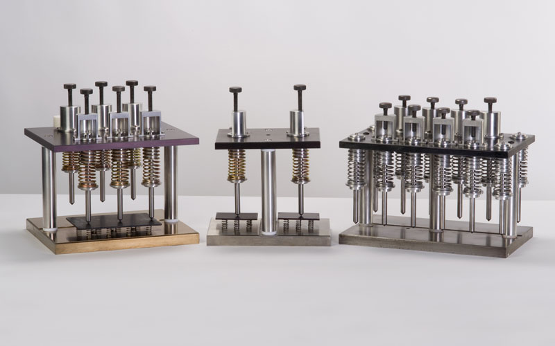
The thin section bonding jig range:
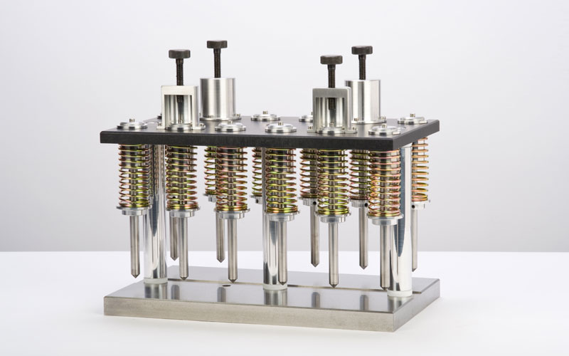
BJ12
The twelve position BJ12 “zero-bonding” jig has two sets of six loading pistons on either side of the central line to enable the jig to accept larger sections if required.  Four bonding stations are equipped with a large section facility which comprises a large area load spreader.  This jig is typically used with two or three workstation rock section lapping systems.  Twelve PTFE load spreaders are supplied with every jig.

BJ9
The six position BJ9 “zero-bonding” jig features two bonding stations.  Using two load spreaders, it is particularly suitable for simultaneously bonding two large format geological thin sections.
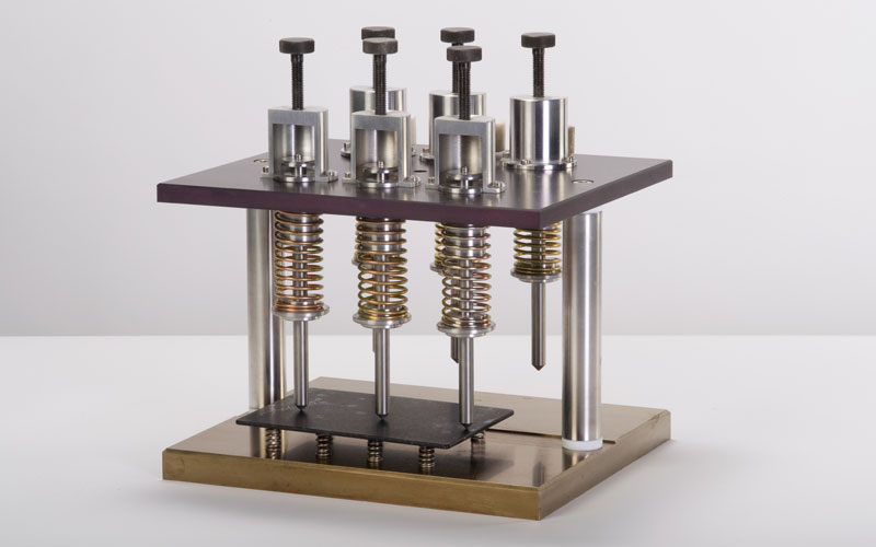
BJ6
The six position BJ6 “zero-bonding” jig is identical to the BJ12 jig but with six pistons.  Two bonding stations are equipped with the large section facility.  Six PTFE load spreaders are supplied with every jig.  This jig is typically used in single workstation geological sample preparation systems or for the bonding of semiconductor wafers.
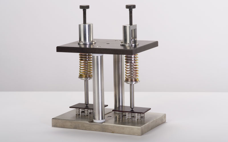
BJ2
This bonding jig is a two piston version of the BJ6.  Both bonding stations can accommodate up to 100mm (4″) diameter samples.  It is ideal for bonding Lithium Niobate (LiNb03) stacks/wafers for subsequent edge lapping and polishing.  The BJ2 includes an aluminium block to ensure the bonding resin is evenly spread.

Visit our Online Consumables store

Download Brochure

Key Features

  • Effective “zero bonding”
  • Controlled thickness bonding
  • Precise bond orientation
  • Large or multiple sample capacity
  • Bonding jigs available for large or small scale operations

Sample capacity:

28 x 48mm 26 x 76mm 35 x 45mm 50 x 76mm 76 x 110mm 102 x 152mm
BJ12 12 12 12 8 4 –
BJ9 6 6 – – 2 2
BJ6 6 6 – 2 2 –
BJ2 2 2 – 2 2 –

Product Specification:

Dimensions Weight
BJ12 307 x 180 x 240mm 12kg
BJ9 260 x 220 x 240mm 9kg
BJ6 152 x 184 x 240mm 6kg
BJ2 152 x 220 x 240mm 6kg

Geological Sciences

geologicalsciences

In many areas of geological study such as mineralogy, petrography and sedimentology you are required to analyse the characteristics of the materials such as soil or rock. To be able to do this a thin section needs to be prepared for microscopic examination.

Logitech precision equipment is ideal for thin or ultra-thin section preparation. Our wide range of versatile systems enable you to trim, lap and polish geological thin sections such as rock, coal, concete and soils.

Each of our systems are fully supported by a wide range of accessories and consumables, such as abrasive powders, polishing cloths and mounting media.

Optoelectronics

optoelectronics

Advances in communication technology have led to the development of a wide variety of optoelectronics and integrated optics devices for applications such as; dense wavelength division multiplexing (DWDM), optical isolators, signal processors and optical switching.

Logitech has a large selection of adaptable systems for the preparation of optoelectronic materials such as; silicon, lithium niobate, lithium tantalate, bismuith silicon oxide, barium titanate and similar materials.

Our systems, accessories and consumables provide defect free face and edge polishing on optoelectronic substrate and scratch free surfaces with exacting and repeatable dimensional tolerances.

Optics

optics

The importance of optical polishing and the processing of optical components has never been greater with the ongoing development of the telecommunications market. Whether for Infra Red and polymer waveguide production or fibre optic cable polishing.

The precision design and manufacture of our equipment enable you to obtain maximum results from the cutting, lapping and polishing of these optical materials.

Mounting Adhesives

Logitech provides a range of mounting media for bonding of semiconductor, optic and geological samples.

Glass Slide Coverslips

Glass coverslips protect valuable thin sections and improve optical clarity for transmitted microscopy.

Glass Microscope Slides

Logitech glass microscope slides are used for the permanent mounting of thin rock, concrete and soil thin sections.

Cleaning Fluids & Powders

Logitech cleaning fluids and powders and non-solvent based. They are suitable for most sample and substrate cleaning applications, including demounting of ultra-thin semiconductor wafers.

the-tech-files

Expert news and views to help sharpen your cutting edge

DIAMONDS ARE AN ENGINEER’S BEST FRIEND

In recent years, diamond has emerged as not only a girl’s best friend, but also as contender as an engineer’s best friend – if the technical challenges of exploiting its remarkable properties can be overcome.

LOGIN TO VIEW

THE END OF THE CHIP FOR SILICON?

Silicon-based semiconducting integrated circuits have changed the world immeasurably over the past 50 years. Today the number of silicon chips in use far outweighs the number of humans currently alive.

LOGIN TO VIEW

OPTIMAL FRICTION FOR OPTIMAL FLATNESS

The wafers used to make semiconducting chips for electronic devices all have one thing in common – they need to be smooth – super smooth. Typically, wafer flatness needs to be controlled within ±2 μm.

FREE TO VIEW
contact-us-icon
contact-us-icon
contact-us-icon

Home  |  Sitemap  |  Privacy Policy  | Cookies Policy | Environmental Policy | Contact Us  |  Extranet | Indicor

We are using cookies to give you the best experience on our website.

You can find out more about which cookies we are using or switch them off in .

Powered by  GDPR Cookie Compliance
Privacy Overview

This website uses cookies so that we can provide you with the best user experience possible. Cookie information is stored in your browser and performs functions such as recognising you when you return to our website and helping our team to understand which sections of the website you find most interesting and useful.

Strictly Necessary Cookies

Strictly Necessary Cookie should be enabled at all times so that we can save your preferences for cookie settings.

If you disable this cookie, we will not be able to save your preferences. This means that every time you visit this website you will need to enable or disable cookies again.