Lapping & Polishing Hard Materials
20th January 2017
PRECISION SYSTEMS BOOST PRODUCTIVITY IN THE PROCESSING OF HARD MATERIALS
The lapping and polishing of hard semiconductor wafers has always been problematic. In a sector centred on high productivity and high quality with demanding industry requirements including; increased material removal rates (MRR), finer and more consistent surface finishes, less sub-surface damage, minimised total thickness variation (TTV), surface roughness and flatness.
Furthermore, working with expensive wafer materials means the process needs to be optimised and repeatable to avoid expensive damage, rework and scrap.
Although lapping and polishing techniques have become more predictable in recent years, the processing of semiconductor wafers often involves significant user expertise and development time to perfect the process and ensure optimal results. Enhanced process control can be attained through the application of Preston’s Law, as this delivers a framework for predicting the amount of material that will be removed in a given time by the lapping and polishing process.
By controlling variables on a precision system that was designed to allow for easy process repeatability, like the PM6 Precision Lapping & Polishing System, process accuracy and high industry standard results can be easily achieved.

PM6 RESULTS
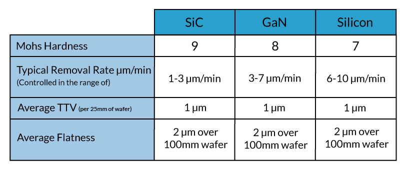
PM6 trials on 100mm substrates across various hard materials has shown the relationship between plate speed and MRR, increased plate speed mean greater MRR. The allowance for easy process repeatability also shows a steady increase in removal rates the more the plates speed increases across the process, in comparison to a machine without the capacity for process repeatability, which can show slightly erratic results meaning increased user input to refine the process.


