Customer Sample Case Study: Advances in Silicon processing
21st March 2018
As one of the most common elements, Silicon is one of the most popular materials used in semiconductor applications. Due to its versatile properties and low band gap this robust material is utilised by many Logitech customers in their device fabrication research.
As a result of our continued collaboration with our customers to optimise their processes, we are continuously seeing advancements in our processes for Silicon and many other popular semiconductor materials.
We recently worked with one of our customers in the ‘Sensing Technologies’ sector to process Silicon on Silicon wafers.
Customer Requirements
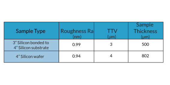
The customer required a collaboration with Logitech to perfect their process on 3″ Silicon wafers bonded to a 4″ Silicon support wafer and also 4″ Silicon wafers (by direct chucking). The samples provided by the customer were required to reach the following specifications:
3″ Silicon bonded to 4″ Silicon Support Wafer for chucking to the vacuum process jig
- Final thickness: 500μm (from ~600μm)
- TTV: <=5μm
4″ Silicon wafers using direct chucking to the vacuum process jig
- Final thickness: 800μm (from ~1000μm)
- TTV: <=5μm
The Process
Throughout the process the decision made by our Process Engineers was to use the Logitech PM6 Precision Lapping & Polishing system for both the lapping and polishing of the wafers. The highly automated features of the PM6 allows operators to reach stringent specifications with minimal user input. Key features such as storing and re-calling multi-stage recipes and Bluetooth data collection and feedback also make for highly analytical and repeatable processes.
Lapping Stage
‘Lapping’ is a material removal process typically involving counter rotating plates and an abrasive with a defined grain sized distribution for effective material removal with minimal surface damage. During the lapping the flatness and micro-roughness of the samples are greatly improved. The lapping plate is shaped to become slightly convex to provide a slightly concave sample, this compensates for the edge rounding that naturally occurs during the CMP polishing process. The plate flatness monitor allows the desired plate shape to be continuously monitored and maintained to minimise any sample to sample variation over time.
The metered abrasive feed feature on the PM6 allows the operator full control of the abrasive delivery to the plate, this results in a reduce in volume of waste for an improvement on cost of ownership.
3″ Silicon bonded on to 4″ Silicon substrate:
Abrasive: Logitech Alumina based lapping abrasive
Plate type: Logitech grooved cast iron lapping plate
Material Removal Rate (MRR): 1-2μm/min
4″ Silicon wafer:
Abrasive: Logitech Alumina based lapping abrasive
Plate type: Logitech grooved glass lapping plate
Material Removal Rate (MRR): 1-2μm/min
Polishing Stage
The final processing stage is Chemical Mechanical Polishing (CMP). Typically this stage results in minimal material removal and removes subsurface damage that may have occurred during the lapping stages.
As the PM6 is a dual lapper and polisher, the full process can be carried out on the one system. It simply involves exchanging the lapping plate for a polishing plate and polishing pad. The PM6 is also available as chemically resistant so is safe to use in chemical polishing processes.
3″ Silicon bonded on to 4″ Silicon substrate:
Abrasive: Logitech polishing solution
Pad type: Logitech grooved Chemcloth polishing pad
Material Removal Rate (MRR): 0.1-0.2μm/min
4″ Silicon wafer:
Abrasive: Logitech polishing solution
Pad type: Logitech grooved Chemcloth polishing pad
Material Removal Rate (MRR): 0.1-0.2μm/min
The Results