Challenging 3D ICs mean changes for CMP processes
3rd March 2016
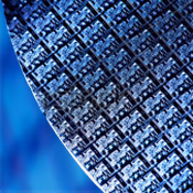
Semiconductor device designers are continuously looking for ways to maximise the number of nodes that fit into each area of semiconducting wafers. CMP processing of 3D stacked logic devices in the form of finFETs and 3D memory can prove more difficult to process than planar ICs. Many more steps are required throughout the process.
An industry standard for processing these stacked devices, or the process of 3D integration using technologies such as through-silicon-vias (TSV), has yet to be set. This has subsequently led to industry experts developing their own technologies and processing tools to determine the best practices for achieving the best results.
Compositional variants from the result of 3D fabrication processes can impact physical properties, therefore affecting CMP process control. Surfaces require almost atomic-levels of control, so we need a better understanding and control over material removal rates and surface uniformity to achieve this whilst controlling the process variants.
This high level of control is incredibly difficult to achieve but essential to ensure processes are as reliable as possible. This allows surface engineers to successfully analyse the process and determine the real influential factures that dictate results. These processes can then be refined and lead to high quality results each process.