Extranet Login

t: +44 (0)1389 875444|e:enquiries@logitech.uk.com

  • Who we are
    • Our History
    • Quality & Accreditations
    • Our Environmental Policies
      • Our WEEE Policy
    • Careers
  • What we offer
    • By application
      • Semiconductors
      • Geological Sciences
      • Optoelectronics
      • Optics
      • Other applications
    • By material
      • Silicon
      • Silicon Carbide
      • Sapphire
      • Gallium Arsenide
      • Cadmium Zinc Telluride
      • Indium Phosphide
      • Rock/Soil
      • Other Materials
  • Products & Solutions
    • Lapping & Polishing
    • Chemical Polishing & Chemical Mechanical Polishing
    • Driven Head Lapping & Polishing Tools
    • Bonding & Impregnation Units
    • Test & Measurement
    • Cutting & Sawing
    • Accessories
    • Consumable Items
    • Consumables Store
  • Knowledge base
    • Whitepapers
    • Tech Files – Blog
    • Technology Transfer Programme
    • Brochures
    • Application Process Notes
    • Case Studies
    • FAQ
  • News & Events
    • News
    • Events
  • Contact
    • How to find us
    • Global Distributors
    • Equipment Returns
Menu
  • Who we are
    • Our History
    • Quality & Accreditations
    • Our Environmental Policies
      • Our WEEE Policy
    • Careers
  • What we offer
    • By application
      • Semiconductors
      • Geological Sciences
      • Optoelectronics
      • Optics
      • Other applications
    • By material
      • Silicon
      • Silicon Carbide
      • Sapphire
      • Gallium Arsenide
      • Cadmium Zinc Telluride
      • Indium Phosphide
      • Rock/Soil
      • Other Materials
  • Products & Solutions
    • Lapping & Polishing
    • Chemical Polishing & Chemical Mechanical Polishing
    • Driven Head Lapping & Polishing Tools
    • Bonding & Impregnation Units
    • Test & Measurement
    • Cutting & Sawing
    • Accessories
    • Consumable Items
    • Consumables Store
  • Knowledge base
    • Whitepapers
    • Tech Files – Blog
    • Technology Transfer Programme
    • Brochures
    • Application Process Notes
    • Case Studies
    • FAQ
  • News & Events
    • News
    • Events
  • Contact
    • How to find us
    • Global Distributors
    • Equipment Returns

Browse:

  • Home
  • Tech Files
  • Automating the challenge of processing fragile wafers

Automating the challenge of processing fragile wafers

Posted in Tech Files

14th July 2015

gaas_wafer_processed_454x314
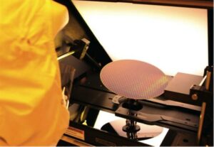
Gallium arsenide (GaAs) has become the substrate material of choice for many electronic devices used in high frequency and optoelectronic applications. However, the processing of GaAs wafers is more difficult than many other substrate materials as it is softer and more fragile.

When processing GaAs wafers, control of the lapping process / plate shape is of paramount importance due to the softness and fragility of the crystal. The lapping plate must be controlled and maintained
 at a specific shape depending on the diameter 
of the wafer.

The shape of the lapping plate deployed has a direct influence on the wafer shape before it enters the polishing stage, where the edge will naturally polish faster than the centre. During lapping, the ultimate aim is to manipulate the wafer shape to an extent that after polishing the wafer is within the flatness specification.

Although manual wafer lapping/polishing tools can meet general manufacturing requirements, the monitoring and control of the plate shape can be laborious. Around 30-60 minutes of conditioning is required for every wafer cycle – and time quickly mounts up when multiple wafers are processed. In an industry that demands high productivity, this is clearly unacceptable.

The only alternative is to seek out a solution that can take care of this function automatically. Tools such as the Akribis-Air from Logitech are able to offer in-situ plate flatness control using an integrated monitor that tracks plate flatness during processing. Software then makes the necessary arm position adjustment to maintain or change plate flatness accordingly until the target shape is attained.

Importantly, the control and maintenance of the plate shape does not require downtime for the plate conditioning cycle, as is the case with manual tools.

To learn more about how automated lapping and polishing systems can aid increase the reliability and efficiency of GaAs processing, download our whitepaper.

If you haven’t already, why not register to receive updates about our forthcoming events.

You will also be able to access:
tech-block
register-now

Home  |  Sitemap  |  Privacy Policy  | Cookies Policy | Environmental Policy | Contact Us  |  Extranet | Indicor

We are using cookies to give you the best experience on our website.

You can find out more about which cookies we are using or switch them off in .

Powered by  GDPR Cookie Compliance
Privacy Overview

This website uses cookies so that we can provide you with the best user experience possible. Cookie information is stored in your browser and performs functions such as recognising you when you return to our website and helping our team to understand which sections of the website you find most interesting and useful.

Strictly Necessary Cookies

Strictly Necessary Cookie should be enabled at all times so that we can save your preferences for cookie settings.

If you disable this cookie, we will not be able to save your preferences. This means that every time you visit this website you will need to enable or disable cookies again.