Automated dynamic lapping for the ultimate substrate finish
20th July 2015
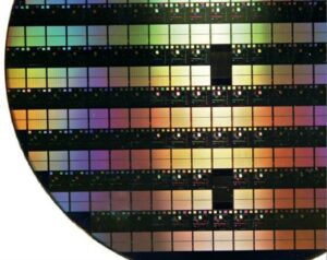 As a result of the extensive and demanding applications for GaAs wafers, there are strict industry requirements for flatness, which typically needs to be within ±2 μm.
Another vital parameter that must be controlled is TTV (total thickness variation) – the difference between the maximum and minimum thickness values of a wafer. Typically this should be within 1 μm per 25 mm for GaAs wafers.
In all cases, a fundamental understanding of the manufacturing process is required to ensure a high quality outcome. Different types of slurries and pads, along with plate speed and jig load all impact the resulting surface. To improve the surface roughness when manufacturing GaAs wafers, a dynamic lapping process can be performed.
Dynamic lapping is when the load starts off high at, say 100 g/cm² and, as the thickness of the GaAs wafer is reduced, the load is also reduced in phases to 75 g/cm², then 50 g/cm², and finally 25 g/cm² before achieving the final lapping target thickness.
The lighter load during the final lapping stages produces a better surface roughness at the end of the lap and therefore reduces the polishing time needed to achieve the target surface roughness, which is typically Ra
To learn more about how Logitech’s automated Akribis-air system can perform this in one continuous operation, download our latest whitepaper.