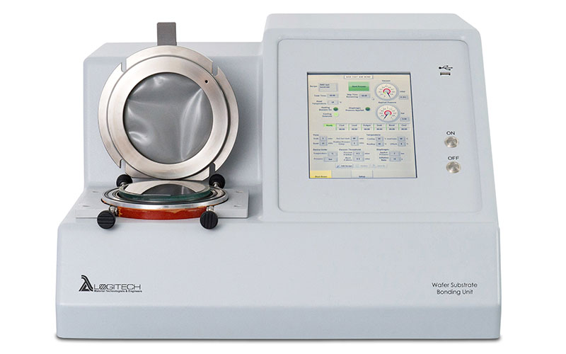
Wafer Substrate Bonding Units
The best materials processing system solutions in the world
Logitech WSBU are premium bonders for the processing of fragile semiconductor wafers such as silicon and gallium arsenide.
If controlling TTV (Total Thickness Variation) is critical to your wafer thinning or polishing process; then it is imperative that the wafer be bonded to a support carrier disc (substrate) to control bond thickness consistency and dimensional accuracy. The Logitech WSBU (Wafer Substate Bonding Units) are designed to achieve the best possible result whilst maintaining sample yield.
These premium bonders are ideal for the processing of fragile and expensive Semiconductor wafers such as Silicon and Gallium Arsenide (GaAs).
The bonding units are designed to minimise breakage with these expensive materials, whilst retaining the highest quality of sample yield.
We offer a wide range of Wafer Substrate Bonding Units (WSBU):
- Single Station, benchtop WSBU with the capacity to bond 100mm (4″) wafers
- Single Station, benchtop WSBU with the capacity to bond 150mm (6″) wafers
- Three Station, benchtop WSBU with the capacity to bond 100mm (4″) wafers
- Three Station, benchtop WSBU with the capacity to bond 150mm (6″) wafers
- Single Station, Standing WSBU with the capacity to bond 300mm (12″) wafers
For more information on our Wafer Substrate Bonding Units please fill in your details in the form and one of our technical experts will get in touch.
Call me back
To speak to one of our technical experts fill this form out and we will get back to you

Logitech Wafer to Substrate Bonding Units (WSBU) provide accuracy and repeatability to meet the needs of the most demanding requirements.
Key Features
- 100mm (4″), 150mm (6″) or 300mm (12″) wafer capacity
- Single or multiple wafer bonding
- Process repeatability
- Automated process cycle
- Excellent wafer to support disc parallelism