
Wafer Thinning & Backlapping
The best materials processing system solutions in the world
Wafer thinning more commonly known as “backlapping” is generally carried out at the end of the device fabrication process.
This reduces the fabricated wafer’s thermal conductivity and speeds up signal transmission across the device.
Typically reducing the wafer thickness from an initial 400-500μm to between 100 and 150μm. However, increasingly sophisticated devices are demanding thinner wafers of 50μm or less. We invest substantial research and development time into the design and production of robust, reliable and accurate systems.
Our Wafer Thinning Machines are:
- Flexible
- Robust
- Intuitive to Use
For more information on how our machines can assist with the wafer thinning process please fill in your details in the form and one of our technical experts will get in touch.
Call me back
To speak to one of our technical experts fill this form out and we will get back to you
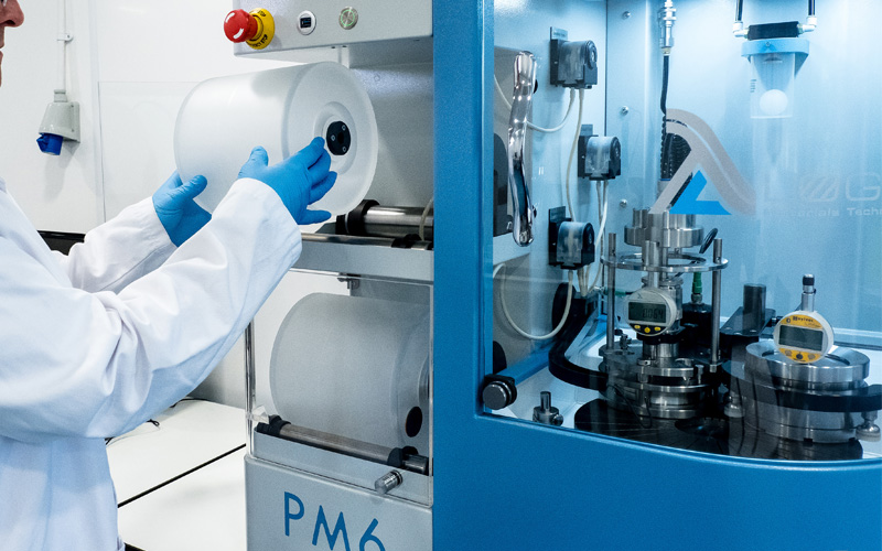
The PM6 is the newest addition to Logitech LTD’s wide range of precision lapping & polishing systems. View the video to see it in action.
Key Features
- Process up to 100mm/4″ wafers
- Up to 100rpm plate speed facilitating faster lapping rates
- Driven jig roller arm with linear sweep
- Bluetooth enabled features
- Automatic plate flatness control


