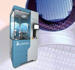
Finishing first – automating wafer lapping and polishing
24th March 2015
 While lapping and polishing processes have become more predictable, there is often significant variation in the results obtained by different operators. Automated systems can remove this variability and help increase productivity, read on to learn more.
Semiconductor wafers are expensive, with custom wafers often costing in excess of $5000.
It is therefore with some incredulity that we find that some chip manufacturers leave the fate of these wafers to processes and technology that involve a significant level of user expertise, guesswork and development time.
Every semiconductor wafer undergoes several common stages during manufacture including slicing the water from the crystal and preparing the surface prior to fabrication using lapping and polishing techniques. After fabrication lapping and polishing processes are again used to thin the devices and remove damage caused during fabrication.
While lapping and polishing processes have become more predictable, there is often significant variation in the results obtained by different operators.
These variations can cause problems as stringent quality requirements dictate that parameters such as total thickness variation (TTV), surface roughness and flatness must be minimised.
It is therefore vital to be able to accurately predict and control the amount of material removed from wafers during a given time.
Preston’s law can be used to analyse the “Prestonian behaviour” of the material removal rate (MRR) and confirm that all-important process stability.
Preston’s equation states that the MRR is proportional to the product of the processing pressure / load / down-force and plate velocity.
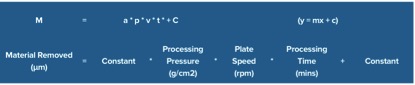
During the typical chemical mechanical polishing processes (CMP) used by the industry, the polishing rate and accuracy are affected not only by the flow of the slurry and the characteristics of the polishing plate, but also by the mechanical action between the wafer and the plate, the chemical action resulting from the chemical components of the slurry, and the interactions between them.
Needless to say, it’s a very skilled job to achieve the precision and surface finish required in demanding wafer applications, due mainly to the required levels of manual set-up and control. It is also time consuming and not conducive to the productivity levels demanded by industry. After all, the search for cost reduction in semiconductor device production is driven by volume and yield.
Automated systems can remove this variability and help increase productivity, to learn more, download our whitepaper.