How to put a sparkle into lapping and polishing sapphire wafers
28th April 2015
 Sapphire substrates are becoming widely used to grow III-V and II-VI compounds such as GaN for LEDs (light-emitting diodes). These are contributing to significant cost and energy savings, meaning that the volume of sapphire wafers being produced has increased dramatically in recent years.
Synthetic sapphire has one of highest hardness values of all materials, after diamond and SiC and this adds to the challenge of processing Sapphire wafers.
The processing stage usually involves a number of chemical mechanical polishing (CMP) steps to generate a super-flat, mirror-like surface with atomic-scale roughness.
The process is typically undertaken using the rotary or orbital motion of a chemical slurry between the wafer and a polishing plate. However, this process can be laborious and it’s a very skilled job to achieve the precision and surface finish required.
This time-consuming process is also subject to user variability and not conducive to the productivity levels demanded by industry.
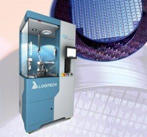
Automated systems, such as Logitech’s Akribis Air, can remove this variability while also increasing productivity. To learn more, download our whitepaper.